PCIE AMBA Integration Guide
1. Introduction
1.1. Introduction
This document is intended to provide guidance on PCIe interface integration into an AMBA based System-On-Chip (SoC). It is assumed that the PCIe interface is connected to the rest of the SoC through an AXI or ACE protocol- based interconnect. The reader is assumed to be conversant with the PCIe, AMBA AXI and AMBA ACE protocols and Arm architecture.
本文档旨在为 PCIe 接口集成到基于 AMBA 的片上系统 (SoC) 提供指导。假设 PCIe 接口通过基于 AXI 或 ACE 协议的互连连接到 SoC 的其余部分。读者应熟悉 PCIe、AMBA AXI 和 AMBA ACE 协议以及 Arm 架构。
The document covers the following topics:
- Description of Terminologies used in this document.
- Guidance on Arm memory type usage for PCIe transactions.
- How to comply with Arm Memory Model Requirements for PCIe transactions from Arm Processing Elements (PEs).
- How to comply with PCIe ordering model in an AMBA based system.
- Topology considerations while integrating PCIe interface into an AMBA based system.
本文档涵盖以下主题:
- 本文档中使用的术语说明
- PCIe 事务的 Arm 内存类型使用指南
- 如何符合 Arm 处理单元 (PE) 生成的 PCIe 事务的 Arm 内存模型要求
- 如何在基于 AMBA 的系统中符合 PCIe 排序模型
- 将 PCIe 接口集成到基于 AMBA 的系统中时的拓扑注意事项
2. Terminology
2.1. Transaction Terminology
A transaction is typically a read or write. The term transaction describes all aspects including the request, any data, and any responses.
事务通常是读或写。事务一词描述了所有方面,包括请求、任何数据和任何响应。
In PCIe a transaction is made up of one or more packets. Each packet travels in one direction only. In AMBA a transaction is made up of one or more transfers. Each transfer travels in one direction only. An AMBA transfer is synonymous with a PCIe packet.
在 PCIe 中,事务由一个或多个数据包组成。每个数据包仅沿一个方向传输。在 AMBA 中,事务由一个或多个传输组成。每个传输仅沿一个方向传输。AMBA 传输与 PCIe 数据包同义。
2.2. Arm Terminology
This document will use terminology as defined in the Arm Architecture Reference Manual [2] for describing the memory type and other memory attributes. This document does not attempt to give a full definition of all the memory types that can be used but gives an overview and describes the different terminology that is used. In keeping with the AMBA AXI and ACE focus of this document, the mapping of Arm memory types and memory attributes to AXI and ACE attributes is provided in sections 3.2 and 3.3.3.
本文档将使用 Arm 架构参考手册 [2] 中定义的术语来描述内存类型和其他内存属性。本文档不试图给出所有可使用的内存类型的完整定义,而是给出概述并描述所使用的不同术语。为了符合本文档的 AMBA AXI 和 ACE 重点,Arm 内存类型和内存属性到 AXI 和 ACE 属性的映射在第 3.2 节和第 3.3.3 节中给出。
Note: In this document, the term “AMBA interconnect” stands for an AXI or ACE protocol-based interconnect. In Arm architecture, memory types can be broadly divided into Device memory types and Normal memory [see section B2.7 in [2]].
注意:在本文档中,“AMBA 互连"一词代表基于 AXI 或 ACE 协议的互连。在 Arm 架构中,内存类型大致可分为 Device 内存类型和 Normal 内存类型 [见第 B2.7 节]。
2.2.1. Device memory
Arm architecture defines the following attributes for Device memory:
- Early Write Acknowledgment: An early acknowledgement for a write transaction can be given before the transaction reaches the peripheral.
- Reordering: Transactions to the same peripheral can be re-ordered with respect to each other.
- Gathering: Multiple transactions can be merged into a single transaction.
Arm 架构为 Device 内存定义了以下属性:
- 早期写响应: 可以在事务到达外设之前给出写事务的早期确认
- 重排序:同一外设的事务可以相互重排序
- 合并:多个事务可以合并成单个事务
Note: Speculative access to Device memory type is never permitted.
注意:永远不允许对 Device 内存类型进行推测性访问。
The Device memory types in ARMv8 are:
| ARMv8 Memory Type | Definition |
|---|---|
| Device-nGnRnE | No Early Write Acknowledgement No Reordering No Gathering |
| Device-nGnRE | Early Write Acknowledgement No Reordering No Gathering |
| Device-nGRE | Early Write Acknowledgement Reordering No Gathering |
| Device-GRE | Early Write Acknowledgement Reordering Gathering |
For accesses to Device memory, the table below shows the different terminology used in ARM v8 and AMBA.
| ARMv8 | AMBA AXI and ACE | Key characteristics of the Arm memory type. |
|---|---|---|
| Device-nGnRnE | Device Non-bufferable (AxCACHE = 0b0000). Same AXI ID. (See Note below) | Response comes from target peripheral. Transactions to the same peripheral must remain in order. |
| Device-nGnRE | Device Bufferable (AxCACHE = 0b0001) Same AXI ID. (See Note below) | Early response is permitted before the transaction has reached the peripheral. (Typically, this only relates to write transactions.) Transactions to the same peripheral must remain in order. |
| Device-nGRE | Device Bufferable (AxCACHE = 0b0001) Re-ordering is not explicit. It is implied by different AXI ID. | Early response is permitted. Transactions to the same peripheral can be re-ordered. |
| Device-GRE | Not supported. Will be treated as Device-nGRE. | Early response is permitted. Transactions to the same peripheral can be re-ordered. Multiple transactions to the same peripheral can be merged into a single transaction. Note: Since AXI/ACE does not support gathering, any merging must be done prior to the transaction entering the AXI/ACE interconnect. |
Note: In AXI using the same AXI ID does not ensure ordering between read and write transactions. To ensure this ordering it is necessary to wait for a response to an early transaction before issuing the later transaction.
注意:在 AXI 中使用相同的 AXI ID 不能确保读和写事务之间的排序。要确保这种排序,必须在发出后续事务之前等待先前事务的响应。
Note: Where it is stated that order is achieved using the same AXI ID, it is also possible to obtain order by ensuring that the later transaction is only issued once the earlier transaction has completed. The later transaction can then be issued using a different AXI ID.
注意:虽然说明中指出使用相同的 AXI ID 可以实现排序,但也可以通过确保后续事务仅在先前事务完成后才发出来实现排序。然后可以使用不同的 AXI ID 发出后续事务。
2.2.2. Normal memory
Normal memory has two key attributes:
- Shareability: Determines the agents/observers in a system that access the same address region.
- Cacheability: Determines if it is permitted to allocate a memory location in a given cache and, if it can be allocated, whether the line is permitted to be dirty (Write-Back) or must be clean (Write-Through).
Normal 内存有两个关键属性:
- 可共享性(Shareability):确定系统中访问同一地址区域的代理/观察者
- 可缓存性(Cacheability):确定是否允许在给定缓存中分配内存位置,如果可以分配,则允许该行是脏的(Write-Back)还是必须是干净的(Write-Through)
Shareability can be one of:
- Non-shareable
- Inner Shareable
- Outer Shareable
Cacheability can be one of:
- Normal Non-cacheable
- Normal Write-Through Cacheable
- Normal Write-Back Cacheable
可共享性可以是以下之一:
- Non-shareable(不可共享)
- Inner Shareable(内部可共享)
- Outer Shareable(外部可共享)
可缓存性可以是以下之一:
- Normal Non-cacheable(普通不可缓存)
- Normal Write-Through Cacheable(普通写通可缓存)
- Normal Write-Back Cacheable(普通写回可缓存)
Cacheability can be defined for both Inner and Outer caches. Inner caches are expected to be within a PE cluster and only the Outer cache memory type is exposed on an AMBA interface. The terms Inner and Outer when used for cacheability are different from the terms Inner and Outer when used for shareability - this is a common source of confusion.
可缓存性可以为内部缓存和外部缓存定义。内部缓存预计在 PE 簇内,只有外部缓存内存类型在 AMBA 接口上公开。当用于可缓存性时,Inner 和 Outer 这两个术语与用于可共享性时的含义不同——这是常见的混淆来源。
For the purposes of this document Inner Cacheability is assumed to be the same as Outer Cacheability. No further use will be made of the terms Inner and Outer to refer to Cacheability and any reference to Inner and Outer later in this document refers to shareability.
为本文档目的,假设 Inner Cacheability 与 Outer Cacheability 相同。本文档将不再使用 Inner 和 Outer 这两个术语来指代可缓存性,本文档中后续任何对 Inner 和 Outer 的引用均指可共享性。
For the purposes of this document it is assumed that Write-Through Cacheable is not supported. This is common for most Arm processor implementations.
为本文档目的,假设不支持 Write-Through Cacheable。这对于大多数 Arm 处理器实现是常见的。
The combination of Inner Shareable and Non-cacheable is not a supported combination. This is because Inner Shareable implies that the location can be held in the cache of another component, so the memory type (that must be compatible between components) cannot be Non-cacheable.
Inner Shareable 和 Non-cacheable 的组合是不支持的组合。这是因为 Inner Shareable 意味着该位置可以保存在另一个组件的缓存中,因此内存类型(必须在组件之间兼容)不能是 Non-cacheable。
If all observers (i.e. requesters) in an Outer Shareable domain are also in the same Inner Shareable domain, then there is no difference between Inner Shareable and Outer Shareable.
如果 Outer Shareable 域中的所有观察者(即请求者)也在同一个 Inner Shareable 域中,则 Inner Shareable 和 Outer Shareable 之间没有区别。
For the rest of this document, Inner Shareable is not considered due to the following reasons:
The difference between Inner and Outer Shareable is deprecated in ACE5, ACE5-Lite, ACE5-LiteDVM, ACE5-LiteACP [see section F5.1 of [1]]. The requirements for Inner Shareable and Outer Shareable are identical and the difference between Inner and Outer Shareable is only in the number of agents that need to be snooped. It is expected that for majority of systems, the Inner and Outer Shareability domains will have the same set of observers. In such cases, the software visible behaviour would be the same regardless of whether shareability attribute is programmed as Inner Shareable or Outer Shareable.
本文档其余部分不考虑 Inner Shareable,原因如下:
Inner 和 Outer Shareable 之间的区别在 ACE5、ACE5-Lite、ACE5-LiteDVM、ACE5-LiteACP 中已弃用 [见第 F5.1 节]。Inner Shareable 和 Outer Shareable 的要求是相同的,Inner 和 Outer Shareable 之间的区别仅在于需要被侦听的代理数量。预计对于大多数系统,Inner 和 Outer Shareability 域将具有相同的观察者集合。在这种情况下,无论可共享性属性被设置为 Inner Shareable 还是 Outer Shareable,软件可见行为都是相同的。
Note: In some AMBA documents, the word “Snoopable” is used instead of “Shareable”. In this document, the word “Shareable” is used throughout.
注意:在某些 AMBA 文档中,使用"Snoopable"一词代替"Shareable”。在本文档中,始终使用"Shareable"一词。
The table below shows the supported combinations of cacheability and shareability that need to be considered.
下表显示了需要考虑的可缓存性和可共享性的支持组合。
| Cacheability | Shareability |
|---|---|
| Non-cacheable | Outer Shareable |
| Write-Back Cacheable | Non-Shareable |
| Write-Back Cacheable | Inner Shareable |
| Write-Back Cacheable | Outer Shareable |
The mapping of permitted combinations of Arm memory type, cacheability and shareability attribute to AMBA AXI attributes [see table A4-5 in section A4.4 of [1]] and ACE attributes [see table D3-3 in section D3.1.1 of [1]] is given in section 3.3 for Inbound transactions and in section 3.2 for Outbound transactions.
允许的 Arm 内存类型、可缓存性和可共享性属性组合到 AMBA AXI 属性 [见第 A4.4 节的表 A4-5] 和 ACE 属性 [见第 D3.1.1 节的表 D3-3] 的映射在第 3.3 节(入站事务)和第 3.2 节(出站事务)中给出。
2.3. PCIe Terminology
The PCIe specification [3] defines the following terminology:
| Term | Definition |
|---|---|
| Downstream | 1. The relative position that is farther from the Root Complex. 2. A direction of information flow where the information is flowing away from the Root Complex. |
| Upstream | 1. The relative position that is closer to the Root Complex. 2. A direction of information flow where the information is flowing towards the Root Complex. |
| Transmitting Port | The Port that transmits the Packet on a given Link. |
| Receiving Port | The Port that receives the Packet on a given Link. |
| Egress Port | The Transmitting Port: that is, the Port that sends outgoing traffic. |
| Ingress Port | The Receiving Port: that is, the Port that accepts incoming traffic. |
| Completer | The PCIe function that completes a request (usually the destination of the request). |
| Relaxed Ordering (RO) and ID based ordering (IDO) | These are packet attribute fields defined in the PCIe specification. The value of these attributes influences the order in which requests and completions arrive at the destination. Refer to the PCIe specification for details [3]. |
Process Address Space ID (PASID)
This is an ID that used to identify the address space of a transaction. Refer to the PCIe specification for details [3].
进程地址空间 ID (PASID):用于识别事务地址空间的 ID。详细说明请参阅 PCIe 规范 [3]。
Fabric
A PCIe fabric is composed of point-to-point links that interconnect a set of components (Endpoints, Switches and Root Complex) [section 1.3 of [3]].
Fabric(结构):PCIe 结构由点对点链路组成,互连一组组件(端点、交换机和根 Complex)
This document will use the following terminology to describe the different aspects of a transaction.
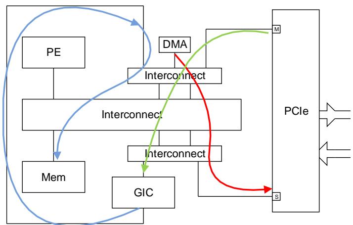
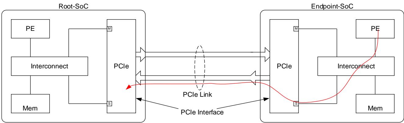
- PCIe Interface is used to describe the IP block that interfaces between an on-chip AMBA system and a PCIe Link. A PCIe Interface will have both AMBA Manager (M) and Subordinate (S) ports. A PCIe Interface could be either a Root Complex or an Endpoint in the PCIe domain.
- Root-SoC is used to describe the SoC that contains the PCIe Root Complex.
- Endpoint-SoC is used to describe an SoC that contains a PCIe Endpoint.
本文档将使用以下术语:
- PCIe 接口:接口于片上 AMBA 系统和 PCIe 链路之间的 IP 块
- Root-SoC:包含 PCIe Root Complex 的 SoC
- Endpoint-SoC:包含 PCIe Endpoint 的 SoC
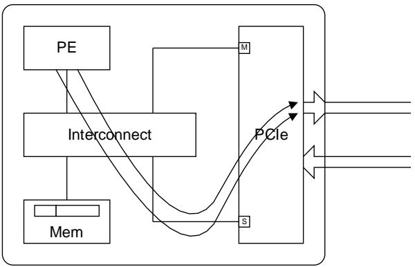
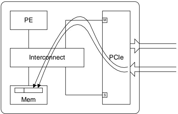
Figure 1 below illustrates the PCIe interface in Root-SoC and Endpoint-SoC
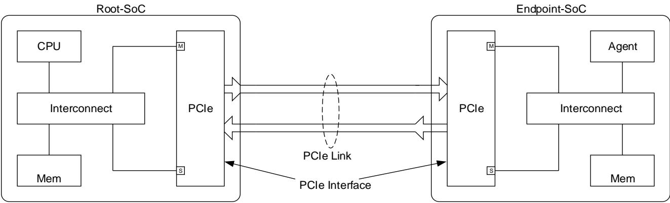
For this document, PCIe switches are not considered.
本文档不考虑 PCIe 交换机
2.3.1. Inbound and Outbound
The terms Outbound and Inbound are used to describe a transaction.
出站(Outbound)和入站(Inbound)用于描述事务
An Outbound transaction has an Outbound Request and (optionally) an Outbound Completion, which returns in the opposite direction. Note that in the case of a completion “Outbound” refers to the direction of the original transaction request, not the direction of the completion.
出站事务具有出站请求和(可选)出站完成,后者沿相反方向返回。请注意,在完成的情况下,“Outbound"指的是原始事务请求的方向,而不是完成的方向。
Likewise, an Inbound transaction has an Inbound Request and (optionally) an Inbound Completion, which returns in the opposite direction. Note that in the case of a completion “Inbound” refers to the direction of the original transaction request, not the direction of the completion.
同样,入站事务具有入站请求和(可选)入站完成,后者沿相反方向返回。请注意,在完成的情况下,“Inbound"指的是原始事务请求的方向,而不是完成的方向。
For a Root-SoC, containing the PCIe Root Complex:
- An Outbound Request travels downstream to the Endpoint.
- An Outbound Completion returns upstream to the Root Complex.
- An Inbound Request travels upstream to the Root Complex.
- An Inbound Completion returns downstream to the Endpoint.
对于 Root-SoC(包含 PCIe Root Complex):
- 出站请求向下游流动到 Endpoint
- 出站完成返回上游到 Root Complex
- 入站请求向上游流动到 Root Complex
- 入站完成返回下游到 Endpoint
For an Endpoint-SoC:
- An Outbound Request travels upstream to the Root Complex.
- An Outbound Completion returns downstream to the Endpoint.
- An Inbound Request travels downstream to the Endpoint.
- An Inbound Completion returns upstream to the Root Complex.
对于 Endpoint-SoC:
- 出站请求向上游流动到 Root Complex
- 出站完成返回下游到 Endpoint
- 入站请求向下游流动到 Endpoint
- 入站完成返回上游到 Root Complex
Note: Care is required when using the terms “upstream” and “downstream”. For example, “arrives from upstream” is the same as “travels downstream”.
注意:使用"upstream"和"downstream"术语时需注意,例如"从上游到达"等同于"向下游流动”
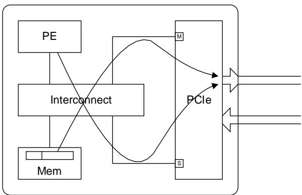
The Figure 2 below shows Inbound and Outbound traffic for a Root-SoC.
下图 2 显示 Root-SoC 的入站和出站流量
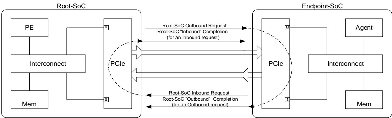
All the examples given in this document are described from the perspective of the Root-SoC.
本文档所有示例均从 Root-SoC 角度描述
3. ARM Memory Type USAGE FOR INBOUND AND OUTBOUND PCIE transactions
3.1. Memory Type Assumptions
The following assumptions are made about the memory type for all transactions.
对所有事务的内存类型做出以下假设
The cacheability of the memory type is the same for all levels of cache. The allocation hints may differ, but the architectural requirements of the memory type are the same.
- Write-Through Cacheable is not supported.
内存类型的可缓存性在所有缓存级别上是相同的。分配提示可能不同,但内存类型的架构要求是相同的。
- 不支持 Write-Through Cacheable。
3.2. Outbound Transaction Memory Type
All Outbound transactions destined for PCIe will have one of the following Arm memory type attributes:
所有发往 PCIe 的出站事务将具有以下 Arm 内存类型属性之一
- Device-nGnRnE
- Device-nGnRE
- Device-nGRE
- Device-GRE
- Normal Non-cacheable
Use of any cacheable memory type is not expected for Outbound transactions. Cache maintenance would be required to ensure visibility of transactions.
不期望对出站事务使用任何可缓存的内存类型。需要进行缓存维护以确保事务的可见性。
Use of cacheable memory is expected for Inbound transaction, see section 3.3 for further details.
期望对入站事务使用可缓存内存,详见第 3.3 节
Table below shows the mapping of Arm memory type to AMBA AXI and ACE memory attributes for Outbound transactions.
下表显示了 Arm 内存类型到出站事务的 AMBA AXI 和 ACE 内存属性的映射。
| Arm memory type and cacheability attribute of the Outbound transaction | Outbound Transaction AXI Memory attributes (AxCACHE) | Outbound Transaction ACE memory attributes (AxCACHE) and shareability domain (AxDOMAIN) |
|---|---|---|
| Device-nGnRnE | Device Non-bufferable | Device Non-bufferable, System |
| Device-nGnRE or Device-nGRE or Device-GRE | Device Bufferable | Device Bufferable, System |
| Normal, Non-cacheable | Normal Non-cacheable Bufferable | Normal Non-cacheable Bufferable, System |
3.3. Inbound Transaction Memory Type
Inbound transactions from the PCIe interface must have appropriate AXI or ACE memory attributes. It is expected that these attributes are derived in a three-step process as follows:
来自 PCIe 接口的入站事务必须具有适当的 AXI 或 ACE 内存属性。这些属性通过三步过程得出,如下所示:
Step 1: The Arm memory type, Cacheability and Shareability attributes of the Inbound transaction is determined.
Step 2: If required, the Cacheability attribute determined in step 1 is overridden based on the transaction’s No Snoop bit value.
Step 3: The Arm memory type and Shareability attribute from step 1 and the cacheability attribute from step 2 is used to determine the AXI or ACE memory attributes of the Inbound transaction.
- 第 1 步:确定入站事务的 Arm 内存类型、可缓存性和可共享性属性
- 第 2 步:如需要,根据事务的 No Snoop 位值覆盖第 1 步确定的可缓存性属性
- 第 3 步:使用第 1 步的 Arm 内存类型和可共享性属性,以及第 2 步的可缓存性属性,确定入站事务的 AXI 或 ACE 内存属性
3.3.1. Step 1: Determining the Arm memory type, cacheability and shareability attributes
For deriving the Arm memory type, cacheability and shareability, the following configurations need to be considered:
为得出 Arm 内存类型、可缓存性和可共享性,需要考虑以下配置:
- The PCIe interface has an associated System Memory Management Unit (MMU) and the System MMU is enabled to provide translations:
In this case, the System MMU must be accessed to get the Arm memory type, cacheability and shareability attributes of the transaction.
- PCIe 接口具有关联的系统内存管理单元 (MMU),且系统 MMU 启用以提供转换:在这种情况下,必须访问系统 MMU 以获取事务的 Arm 内存类型、可缓存性和可共享性属性。
- PCIe interface does not have an associated System MMU or the System MMU is bypassed or disabled: In this configuration, the PCIe interface must be able to determine the Arm memory type, cacheability and shareability attributes of the location an Inbound transaction is targeting. Typically, this can be done using a primitive address decode to associate specific address ranges with specific Arm memory type, cacheability and shareability attributes. It is expected that this association is configurable to allow maximum flexibility.
- PCIe 接口没有关联的系统 MMU 或系统 MMU 被绕过或禁用:在这种配置下,PCIe 接口必须能够确定入站事务目标位置的 Arm 内存类型、可缓存性和可共享性属性。通常,可以使用原始地址解码将特定地址范围与特定 Arm 内存类型、可缓存性和可共享性属性关联起来。预计这种关联是可配置的,以允许最大的灵活性。
It is expected that the Arm memory type for a location that is in a peripheral is determined based on the properties of the location, as defined in the Arm Architecture reference manual [see section B2.7.1 and B2.7.2 of [2]].
预计外设中位置的 Arm 内存类型将根据位置的属性确定,详见 Arm 架构参考手册。
It is strongly recommended that DRAM memory is mapped as Normal memory with Write-Back as the cacheability attribute.
强烈建议将 DRAM 内存映射为具有 Write-Back 作为可缓存性属性的 Normal 内存。
Note: The constraint to be considered while setting the memory type of a location is that the weakest memory type that can be used is determined by the properties of the location. It is permitted to use a stronger memory type although it might not be performance optimal.
注意:设置位置的内存类型时需要考虑的约束是,可以使用 的最弱内存类型由位置的属性决定。允许使用更强的内存类型,尽管可能不是最佳性能。
3.3.2. Step 2: Modifying the cacheability attribute based on the transaction’s No Snoop bit value
The “No Snoop” bit is a transaction attribute provided by PCIe specification for a requester to indicate whether hardware coherency management is expected or not [see section 2.2.6.5 and 7.5.3.4 of [3]].
“No Snoop"位是 PCIe 规范提供的事务属性,用于指示请求者是否期望硬件一致性管理
For an SoC with software visible caches, the cacheability attribute of the transaction must be forced to Non-cacheable if “No Snoop” bit for the transaction is 1 and the Arm memory type (determined in step 1) is Normal.
对于具有软件可见缓存的 SoC,如果事务的"No Snoop"位为 1 且 Arm 内存类型(第 1 步确定)为 Normal,则必须将可缓存性属性强制为 Non-cacheable
For an SoC where all caches are software invisible, it is strongly recommended that cacheability attribute of the transaction is set to Non-cacheable if “No Snoop” bit for the transaction is 1 and the Arm memory type (determined in step 1) is Normal.
对于所有缓存都是软件不可见的 SoC,强烈建议如果事务的"No Snoop"位为 1 且 Arm 内存类型为 Normal,则将可缓存性属性设置为 Non-cacheable
In both cases, if the “No Snoop” bit is 0, then the cacheability attribute from step 1 is retained.
在这两种情况下,如果"No Snoop"位为 0,则保留第 1 步的可缓存性属性
3.3.3. Step 3: Mapping the Arm memory type, cacheability and shareability attributes to AXI/ACE memory attributes
In this step, Arm memory type and shareability attributes from Step 1 and the cacheability attribute from step 2 is mapped to AXI or ACE memory attributes prior to issuing into the AMBA interconnect.
在此步骤中,将第 1 步的 Arm 内存类型和可共享性属性以及第 2 步的可缓存性属性映射到 AXI 或 ACE 内存属性,然后发送到 AMBA 互连
The table below provides the mapping information:
- AMBA AXI memory attribute [see table A4-5 in section A4.4 of [1]] for the transaction given its final Arm memory type, cacheability attribute, shareability attribute.
- AMBA ACE memory attributes [see table D3-3 in section D3.1.1 of [1]] for the transaction given its final Arm memory type, cacheability attribute, shareability attribute.
- AMBA AXI 内存属性 [见第 A4.4 节的表 A4-5]:根据事务的最终 Arm 内存类型、可缓存性属性和可共享性属性
- AMBA ACE 内存属性 [见第 D3.1.1 节的表 D3-3]:根据事务的最终 Arm 内存类型、可缓存性属性和可共享性属性
Note: As explained in section 2.2.2, this section only considers Outer Shareable.
注意:如第 2.2.2 节所述,本节仅考虑 Outer Shareable
| Inbound PCIe transaction: Arm memory type, cacheability and shareability attributes (after Step 2) | PCIe Transaction AXI Memory attribute (excluding the allocate attributes) | PCIe Transaction ACE memory attribute (excluding the allocate attributes) and shareability domain |
|---|---|---|
| Device-nGnRnE | Device Non-bufferable | Device Non-bufferable, System |
| Device-nGnRE or Device-nGRE or Device-GRE | Device Bufferable | Device Bufferable, System |
| Normal, Write-Back, Outer Shareable | WriteBack | WriteBack, Outer Shareable |
| Normal, Non-cacheable, Outer Shareable | Normal Non-cacheable, Bufferable | Normal Non-cacheable Bufferable, System |
3.3.4. Coherency management for Inbound transactions
For an Inbound PCIe transaction, the table below provides the following information:
- For a given location, possible combinations of the Inbound PCIe transaction attributes (after step 2 - see section 3.3.2 and PE side attributes for exchanging data between Software running on a PE and a PCIe Requester.
- Whether or not software cache maintenance is required to maintain coherency.
- The AXI and ACE attributes corresponding to the Inbound PCIe transaction attributes.
对于入站 PCIe 事务,下表提供以下信息:
- 对于给定位置,入站 PCIe 事务属性(第 2 步后)与 PE 侧属性的可能组合
- 是否需要软件缓存维护来保持一致性
- 与入站 PCIe 事务属性相对应的 AXI 和 ACE 属性
Note: As explained in section 2.2.2, this section only considers Outer Shareable.
| PE transaction: Arm memory type, cacheability and shareability attributes | Inbound PCIe transaction: Arm memory type, cacheability and shareability attributes (after step 2 -i.e. after considering No Snoop attribute) | Coherency Management | PCIe Transaction AXI Memory attribute (excluding the allocate attributes) attributes) | PCIe Transaction ACE memory attribute (excluding the allocate attributes) and shareability domain |
|---|---|---|---|---|
| Normal, Write-Back, Outer Shareable | Normal, Write-Back, Outer Shareable | Hardware managed. | WriteBack | WriteBack, Outer Shareable |
| Normal, Write-Back, Non-shareable | Normal, Write-Back, Outer Shareable | Software cache maintenance (This assumes that PE transaction looks up the cache in which PCIe transaction might be cached). | WriteBack | WriteBack, Outer Shareable |
| Normal, Non-cacheable, Outer Shareable | Normal, Write-Back, Outer Shareable | Not permitted unless all caches in the system are invisible to software. With software invisible caches, hardware would ensure coherence. | WriteBack | WriteBack, Outer Shareable |
| Normal, Write-Back, Outer Shareable | Normal, Non-cacheable, Outer Shareable | Software cache maintenance unless all caches in the system are invisible to software. With software invisible caches, hardware would ensure coherence. | Normal Non-cacheable, Bufferable | Normal Non-cacheable Bufferable, System |
| Normal, Write-Back, Non-shareable | Normal, Non-cacheable, Outer Shareable | Software cache maintenance | Normal Non-cacheable, Bufferable | Normal Non-cacheable Bufferable, System |
| Normal, Non-cacheable, Outer Shareable | Normal, Non-cacheable, Outer Shareable | Not cached. | Normal Non-cacheable, Bufferable | Normal Non-cacheable Bufferable, System |
For a location which is mapped as one of the Device memory types for both the PE transaction and the PCIe Inbound transaction, there is no hardware or software cache maintenance required as Device memory type locations are never cached. The Device memory type assigned to the location on the PE side can be different from the Device memory type assigned to the location on the PCIe Inbound side. However, software (or a combination of software and firmware) is responsible for ensuring that both PE transaction and PCIe Inbound transaction uses a Device memory type that matches with the properties of the target location.
对于 PE 事务和 PCIe 入站事务都将位置映射为 Device 内存类型之一的情况,不需要硬件或软件缓存维护,因为 Device 内存类型位置永远不会被缓存。分配给 PE 侧位置的 Device 内存类型可以与分配给 PCIe 入站侧位置的 Device 内存类型不同。但是,软件(或软件和固件的组合)负责确保 PE 事务和 PCIe 入站事务都使用与目标位置属性相匹配的 Device 内存类型。
It is expected that software (or the combination of software and firmware) will not map a location as Normal memory for the PE transaction and map the same location as Device memory for the PCIe Inbound transaction. Similarly, it is expected that software (or the combination of software and firmware) will not map a location as Device memory for the PE transaction and map the same location as Normal memory for the PCIe Inbound transaction. If software (or the software-firmware combination) behaves contrary to these expectations, then it is software’s (or the software-firmware combination’s) responsibility to manage the errors that can happen due to such a mapping.
期望软件(或软件和固件的组合)不会将某个位置映射为 PE 事务的 Normal 内存同时将同一位置映射为 PCIe 入站事务的 Device 内存。同样,期望软件不会将某个位置映射为 PE 事务的 Device 内存同时将同一位置映射为 PCIe 入站事务的 Normal 内存。如果软件(或软件-固件组合)的行为与这些预期相反,则软件(或软件-固件组合)负责管理由于这种映射可能导致的错误。
Note: With software invisible caches, the assumption is that hardware would ensure coherence by accessing the caches regardless of the cacheability and shareability attributes.
注意:对于软件不可见缓存,假设硬件将通过访问缓存来确保一致性,而不考虑可缓存性和可共享性属性
4. COMPLYING TO ARM memory model FOR PE GENERATED PCIE TRANSACTIONS
符合 ARM 内存模型以用于 PE 生成的 PCIE 事务
PE generated PCIe transactions are Outbound transactions for a Root-SoC and for an Endpoint-SoC.
PE 生成的 PCIe 事务对于 Root-SoC 和 Endpoint-SoC 都是出站事务。
This section describes the following:
- Arm memory type mapping options for PCIe address spaces.
- Requirements that the PCIe interface, the SoC interconnect and the PE must meet to preserve Arm memory model’s guarantees.
- End to end ordering guarantees provided by the system for a PE request targeting a PCIe completer.
本节内容如下:
- 针对 PCIe 地址空间的 Arm 内存类型映射选项。
- PCIe 接口、SoC 互连和 PE 必须满足的要求,以确保 Arm 内存模型的保证得以保留。
- 系统为目标是 PCIe completer 的 PE 请求提供的端到端排序保证。
From a PE perspective, all memory locations in a PCIe completer will be mapped in the PE’s translation tables as one of the following:
- Device-nGnRnE.
- Device-nGnRE.
- Device-nGRE.
- Device-GRE.
- Normal with Non-cacheable as the cacheability attribute.
从 PE 的角度来看,PCIe completer 中的所有内存位置将在 PE 的转换表中映射为以下之一:
- Device-nGnRnE
- Device-nGnRE
- Device-nGRE
- Device-GRE
- Normal with Non-cacheable(作为可缓存性属性)
Sections 4.1,4.2 and 4.3 details the requirements to be met for preserving the guarantees given to software for each Arm memory type.
第 4.1、4.2 和 4.3 节详细说明了为保持对每种 Arm 内存类型给予软件的保证而要满足的要求。
4.1. Device-nGnRnE and Device-nGnRE
For Device-nGnRnE and Device-nGnRE memory types, the Endpoint arrival order must match program order and read speculation is not permitted.
对于 Device-nGnRnE 和 Device-nGnRE 内存类型,Endpoint 到达顺序必须与程序顺序匹配,并且不允许 Read Speculation
The nGnRnE memory type can be used to target the configuration, prefetchable and non-prefetchable PCIe address spaces.
nGnRnE 内存类型可用于寻址配置、可预取和不可预取 PCIe 地址空间。
The nGnRE memory type can be used to target the prefetchable and non-prefetchable PCIe address spaces.
nGnRE 内存类型可用于寻址可预取和不可预取 PCIe 地址空间。
Note: Writes to prefetchable and non-prefetchable memory space of a PCIe completer are posted
对 PCIe Completer 的可预取和不可预取内存空间的写入是 Posted 的
- i.e. the completer will not send a response back to the requester. Despite the lack of an explicit response back from the completer, the Arm architecture permits mapping the prefetchable and non-prefetchable memory spaces as Device-nGnRnE [see section E.2.7.2 of [2]]. There are no restrictions on mapping the prefetchable and non-prefetchable memory spaces as Device-nGnRE.
即 Completer 不会向请求者发送响应。尽管 Completer 没有明确的响应,但 Arm 架构允许将可预取和不可预取内存空间映射为 Device-nGnRnE [see section E.2.7.2 of [2]]. 将可预取和不可预取内存空间映射为 Device-nGnRE 没有限制。
4.1.1. PE and Interconnect requirements for handling Outbound requests to Device-nGnRnE or Device-nGnRE mapped locations
PE 和互连处理目标为 Device-nGnRnE 或 Device-nGnRE 映射位置的出站请求的要求
For ensuring that Device-nGnRnE and Device-nGnRE memory type works correctly, the PE and the interconnect needs to meet the following requirements:
- Transactions to a location mapped as Device-nGnRnE must have “Device Non-bufferable” as the AXI memory type. For ACE, the memory type is “Device Non-bufferable” with “System” as the shareability domain.
- Transactions to a location mapped as Device-nGnRE must have “Device Bufferable” or “Device Non-bufferable” as the AXI memory type. For ACE, the memory type is “Device Bufferable” or “Device Non-bufferable” with “System” as the shareability domain.
- If there is a read request outstanding to a peripheral, then any new read request to the same peripheral must use the same AXI ID as that of the outstanding read.
- If there is a write request outstanding to a peripheral, then any new write request to the same peripheral must use the same AXI ID as that of the outstanding write.
- Determination of which peripheral region an Outbound PE request falls into is done by implementation defined methods. If such a determination is not possible, then it must be assumed that all Device Bufferable and Device Non-bufferable transactions from a PE are to the same peripheral region and must obey the AXI ID requirements stated above.
- AMBA interconnect does not guarantee any order between read and write transactions. Therefore, to preserve program order between reads and writes, the PE needs to wait for completion of previously issued read transactions to a given peripheral before issuing write transactions to the same peripheral and vice versa.
为确保 Device-nGnRnE 和 Device-nGnRE 内存类型正常工作,PE 和互连需要满足以下要求:
- 映射为 Device-nGnRnE 的位置的事务,其 AXI 内存类型必须为“Device Non-bufferable”。对于 ACE,内存类型为“Device Non-bufferable”,共享域为“System”。
- 映射为 Device-nGnRE 的位置的事务,其 AXI 内存类型必须为“Device Bufferable”或“Device Non-bufferable”。对于 ACE,内存类型为“Device Bufferable”或“Device Non-bufferable”,共享域为“System”。
- 如果存在对某个外设的未完成读取请求,则对同一外设的任何新读取请求必须使用与该未完成读取相同的 AXI ID。
- 如果存在对某个外设的未完成写入请求,则对同一外设的任何新写入请求必须使用与该未完成写入相同的 AXI ID。
- 确定出站 PE 请求属于哪个 Peripheral 区域由实现定义的方法完成。如果无法进行此类确定,则必须假定来自 PE 的所有 Device Bufferable 和 Device Non-bufferable 事务都指向同一 Peripheral 区域,并且必须遵守上述 AXI ID 要求。
- AMBA 互连不保证读写事务之间的任何顺序。因此,为了保持读写之间的程序顺序,PE 需要等待先前发往给定外设的读取事务完成,然后才能向同一外设发出写入事务,反之亦然。
4.1.2. PCIe interface requirements for handling Outbound requests to Device-nGnRnE or Device-nGnRE mapped locations
PCIe 接口处理目标为 Device-nGnRnE 或 Device-nGnRE 映射位置的出站请求的要求
For the PCIe interface, requests to a Device-nGnRnE mapped location would be received with “Device Non-bufferable” attribute from the AMBA interconnect. Requests to a Device-nGnRE mapped location would be received with “Device Bufferable” attribute from the AMBA interconnect.
对于 PCIe 接口,目标为 Device-nGnRnE 映射位置的请求将从 AMBA 互连接收到“Device Non-bufferable”属性。目标为 Device-nGnRE 映射位置的请求将从 AMBA 互连接收到“Device Bufferable”属性。
On top of being compliant with the PCIe ordering model (see section 5 for the rules) and the AMBA specification [1], the PCIe interface needs to meet the following requirements:
- Read transactions can get re-ordered with respect to program order while traversing the PCIe fabric. Therefore, the PCIe interface must send out a Device Non-bufferable or Device Bufferable read only after completion has been received for earlier read transactions with the same AXI ID targeting the same peripheral region [for definition of peripheral region see section A6.2 of [1]].
- Configuration writes can get re-ordered with respect to program order while traversing the PCIe fabric. Therefore, the PCIe interface must send out a Device Non-bufferable configuration write only after completion has been received for earlier configuration writes with the same AXI ID targeting the same peripheral region.
- Posted writes with Device Bufferable or Device Non-bufferable attribute targeting the same peripheral region (i.e. having the same AXI ID) must not be allowed to overtake each other while transiting through the PCIe interface to the PCIe link.
- Note that this applies even if one write has Device Bufferable attribute and the second write has Device Non-bufferable attribute.
- For configuration writes, the PCIe interface must return the write completion response to the requester only after completion from the PCIe completer has been received.
- RO must not be set for transactions with the Device Bufferable or Device Non-bufferable attribute.
- IDO attribute is not set for any transaction from a PE or if IDO is set for transactions from a PE, then all requests from that PE has the same PCIe Requester ID and same PASID.
- It is expected that PASID will be set only for Outbound transactions from an Endpoint-SoC.
- It is expected that all transactions from a Root-SoC PE would have the same PCIe Requester ID.
除了符合 PCIe 排序模型和 AMBA 规范之外,PCIe 接口还需要满足以下要求:
- 读事务在遍历 PCIe 结构时,相对于程序顺序可能会被乱序。因此,PCIe 接口必须仅在收到针对同一外设区域的、具有相同 AXI ID 的较早读取事务的完成之后,才能发出 Device Non-bufferable 或 Device Bufferable 读。
- 配置写在遍历 PCIe 结构时,相对于程序顺序可能会被乱序。因此,PCIe 接口必须仅在收到针对同一外设区域的、具有相同 AXI ID 的较早配置写的完成之后,才能发出 Device Non-bufferable 配置写。
- 具有 Device Bufferable 或 Device Non-bufferable 属性的 Posted 写,如果目标是同一外设区域(即具有相同的 AXI ID),则在通过 PCIe 接口传输到 PCIe 链路时,不得相互越过。
- 请注意,即使其中一个写具有 Device Bufferable 属性而另一个写具有 Device Non-bufferable 属性,此规则也适用。
- 对于配置写,PCIe 接口必须仅在收到来自 PCIe Completer的完成之后,才能将写完成响应返回给请求者。
- 对于具有 Device Bufferable 或 Device Non-bufferable 属性的事务,不得设置 RO。
- PE 发出的任何事务均不得设置 IDO 属性;或者,如果为 PE 发出的事务设置了 IDO,则该 PE 的所有请求必须具有相同的 PCIe 请求者 ID 和相同的 PASID。
- 预计 PASID 将仅为 Endpoint-SoC 发出的出站事务设置。
- 预计 Root-SoC PE 发出的所有事务都将具有相同的 PCIe 请求者 ID。
4.1.3. Example use cases for Device-nGnRnE and Device-nGnRE mapping of PCIe address spaces
The most important use case for Device-nGnRnE mapping is configuration writes. This is illustrated by the following example:
If we imagine a case where software writes to a configuration register and then reads a prefetchable BAR space location whose value depends on the configuration register, then it is important that the software does the read only after it knows that the configuration write has reached the target and is complete. The only way for software to know that a configuration write is complete is to make sure that the configuration write uses the Device-nGnRnE attribute and have a DSB between the configuration write and the read.
Device-nGnRnE 映射最重要的用例是配置写。以下示例对此进行了说明: 如果我们设想一个场景,软件写入一个配置寄存器,然后读取一个可预取 BAR 空间位置,该位置的值取决于配置寄存器,那么重要的是,软件只有在知道配置写已到达目标并完成之后才执行读取。软件知道配置写完成的唯一方法是确保配置写使用 Device-nGnRnE 属性,并在配置写和读取之间设置一个 DSB。
Secondly, the Device-nGnRnE and Device-nGnRE types provide the ability to pipeline transactions to PCIe targets even if those transactions need to arrive in program order at the target. This illustrated by the following examples:
- Two read transactions, the first of which is a read from the receive buffer and the second of which is a read from the buffer status register, are required to remain in program order to give the correct behaviour. If the transactions are re-ordered on the PCIe fabric then it would be possible to read a status register which indicates that the receive buffer still contains entries when, in reality, the buffer will be emptied by the read from the receive buffer. In this scenario, if both transactions have the Device-nGnRnE or Device-nGnRE attribute, then they will arrive in program order at the target as desired even if they are pipelined.
- A similar situation exists for two Outbound configuration write requests. An example would be software needing to write to Device Control register to set the Max Payload size of write requests by a Device prior to doing a second configuration write to set the Bus Master Enable bit in the Device’s Command register. In this case, it is necessary that the first configuration write arrives at the Device before the second configuration write for correct operation. In this scenario, if both transactions have the Device-nGnRnE attribute, then they will arrive in order program order at the target as desired even if they are pipelined.
其次,Device-nGnRnE 和 Device-nGnRE 类型提供了将事务流水线化到 PCIe 目标的能力,即使这些事务需要在目标处按程序顺序到达。以下示例对此进行了说明:
- 两个读取事务,第一个是从接收缓冲区读取,第二个是从缓冲区状态寄存器读取,需要保持程序顺序才能确保正确的行为。如果事务在 PCIe 结构上被乱序,那么可能会读取到一个状态寄存器,该寄存器指示接收缓冲区仍然包含条目,而实际上,缓冲区将因从接收缓冲区的读取而清空。在这种情况下,如果两个事务都具有 Device-nGnRnE 或 Device-nGnRE 属性,那么即使它们是流水线化的,它们也将按预期按程序顺序到达目标。
- 对于两个出站配置写请求,也存在类似情况。一个例子是软件需要写入设备控制寄存器以设置设备的写请求最大载荷大小,然后才进行第二次配置写以设置设备命令寄存器中的总线主控使能位。在这种情况下,为了正确操作,第一个配置写必须在第二个配置写之前到达设备。在这种情况下,如果两个事务都具有 Device-nGnRnE 属性,那么即使它们是流水线化的,它们也将按预期按程序顺序到达目标。
4.2. Device-nGRE and Device-GRE
For Device-nGRE and Device-GRE memory types, read speculation is not permitted. However, it is permitted for the arrival order of transactions at the destination peripheral to be different from program order except for transactions targeting the same location (see section 4.4. Complying with internal visibility requirement of the Arm memory model).
对于 Device-nGRE 和 Device-GRE 内存类型,不允许 Read Speculation。但是,允许事务在目标外设的到达顺序与程序顺序不同,但目标为同一位置的事务除外。
Any gathering permitted by the Device-GRE memory type must occur prior to entering the AXI or ACE interconnect. This is because AXI and ACE does not support signalling of gathering via attributes.
Device-GRE 内存类型允许的任何 Gathering 必须在进入 AXI 或 ACE 互连之前发生。这是因为 AXI 和 ACE 不支持通过属性来指示。
Device-nGRE memory type can be used to target non-prefetchable and prefetchable PCIe address spaces.
Device-nGRE 内存类型可用于寻址不可预取和可预取 PCIe 地址空间。
Device-GRE memory type can be used to target prefetchable PCIe address space.
Device-GRE 内存类型可用于寻址可预取 PCIe 地址空间。
On AXI interconnect, transactions targeting locations mapped with these types will have “Device Bufferable” as the memory type. For ACE, the memory type is “Device Bufferable” and the shareability domain is “System”.
在 AXI 互连上,目标为这些类型映射位置的事务,其内存类型将为“Device Bufferable”。对于 ACE,内存类型为“Device Bufferable”,共享域为“System”。
The only restriction on usage of AXI IDs is that transactions to the same address must have the same AXI ID if multiple such transactions are outstanding concurrently. The rules for handling two transactions to the same address is given in 4.4.
AXI ID 使用的唯一限制是,如果存在多个同时未完成的事务,则目标为同一地址的事务必须具有相同的 AXI ID。处理目标为同一地址的两个事务的规则在 4.4. Complying with internal visibility requirement of the Arm memory model 节中给出。
4.2.1. PCIe interface requirements for handling Outbound requests to Device-nGRE and Device-GRE mapped locations
Requests to a Device-nGRE or Device-GRE mapped location would be received with “Device Bufferable” attribute from the AMBA interconnect by the PCIe interface.
目标为 Device-nGRE 或 Device-GRE 映射位置的请求将从 AMBA 互连接收到"Device Bufferable"属性。
On top of being compliant with the PCIe ordering model (see section 5 for the rules) and the AMBA specification [1], the requirements in section 4.4, section 4.5 and section 4.6 apply.
除了符合 PCIe 排序模型和 AMBA 规范之外,第 4.4、4.5 和 4.6 节的要求也适用。
Note: It is a software error to map configuration space as Device-nGRE or Device-GRE (see section 4.8, note 1). With such a mapping, program order arrival of configuration accesses will not be guaranteed by the system. If configuration space is mapped as Device-nGRE or Device-GRE, the PCIe interface is not expected to send out configuration reads or configuration writes one at a time unless they have the same AXI ID.
注意:将配置空间映射为 Device-nGRE 或 Device-GRE 是软件错误(见第 4.8 节注释 1)。使用这种映射,系统将不保证配置访问的到达顺序。如果配置空间被映射为 Device-nGRE 或 Device-GRE,PCIe 接口预计不会一次发送一个配置读或配置写,除非它们具有相同的 AXI ID。
4.3. Normal with Non-cacheable as the cacheability attribute
For the Normal memory type, read speculation is permitted and the Endpoint arrival order of transactions can be different from program order except for transactions targeting the same location (see section 4.4). It is expected that this memory type is only used to target an address space that is prefetchable.
对于 Normal 内存类型,允许读推测,事务在 Endpoint 的到达顺序可以与程序顺序不同,但目标为同一位置的事务除外。预计此内存类型仅用于寻址可预取的地址空间。
Transactions targeting Normal memory type locations with Non-cacheable attribute will have “Normal Noncacheable Bufferable” as the AXI memory type. For ACE, the memory type is “Normal Non-cacheable Bufferable” and the Shareability domain is “System”.
目标为具有 Non-cacheable 属性的 Normal 内存类型位置的事务,其 AXI 内存类型将为"Normal Noncacheable Bufferable”。对于 ACE,内存类型为"Normal Non-cacheable Bufferable”,共享域为"System"。
The only restriction on usage of AXI IDs is that transactions to the same address must have the same AXI ID if multiple such transactions are outstanding concurrently. The rules for handling two transactions to the same address is given in 4.4.
AXI ID 使用的唯一限制是,如果存在多个同时未完成的事务,则目标为同一地址的事务必须具有相同的 AXI ID。处理目标为同一地址的两个事务的规则见第 4.4 节。
4.3.1. PCIe interface requirements for handling Outbound requests to Normal Non-cacheable mapped memory locations
Requests to a Normal memory type location with the Non-cacheable attribute would be received with “Normal Non-cacheable Bufferable” attribute from the AMBA interconnect by the PCIe interface.
目标为具有 Non-cacheable 属性的 Normal 内存类型位置的请求将从 AMBA 互连接收到"Normal Non-cacheable Bufferable"属性。
On top of being compliant with the PCIe ordering model (see section 5 for the rules) and the AMBA specification [1], the requirements in section 4.4, section 4.5 and section 4.6 apply.
除了符合 PCIe 排序模型和 AMBA 规范之外,第 4.4、4.5 和 4.6 节的要求也适用。
Note: It is a software error to map configuration space as Normal Non-cacheable (see section 4.8, note 1). With such a mapping, program order arrival of configuration accesses will not be guaranteed by the system. If configuration space is mapped as Normal Non-cacheable, the PCIe interface is not expected to send out configuration reads or configuration writes one at a time unless they have the same AXI ID.
注意:将配置空间映射为 Normal Non-cacheable 是软件错误(见第 4.8 节注释 1)。使用这种映射,系统将不保证配置访问的到达顺序。如果配置空间被映射为 Normal Non-cacheable,PCIe 接口预计不会一次发送一个配置读或配置写,除非它们具有相同的 AXI ID。
Note: If software maps non-prefetchable space as Normal Non-cacheable, then it is the responsibility of software to deal with the consequences of speculative accesses to non-prefetchable space. The PCIe interface is not expected to flag an error if a request with “Normal Non-cacheable Bufferable” attribute is targeting the nonprefetchable space. It is expected that the PCIe interface would forward such requests to the completer in the same way as it would forward a “Normal Non-cacheable Bufferable” request targeting the prefetchable space.
注意:如果软件将不可预取空间映射为 Normal Non-cacheable,则软件有责任处理对不可预取空间进行推测性访问的后果。如果具有"Normal Non-cacheable Bufferable"属性的请求目标是不可预取空间,PCIe 接口预计不会标记错误。PCIe 接口预计将以与转发目标为可预取空间的"Normal Non-cacheable Bufferable"请求相同的方式转发此类请求。
4.4. Complying with internal visibility requirement of the Arm memory model
Internal visibility requirement of the Arm memory model [see section B2.3.3 of [1]] requires that all accesses from a PE to the same location happens in program order.
Arm 内存模型的内部可见性要求要求 PE 对同一位置的所有访问都按程序顺序发生。
To comply with this requirement, the PE and the interconnect must comply with the following requirements:
- If there is a write request outstanding from a PE to a given location, then any new write request to that location from the same PE must use the same AXI ID as that of the outstanding write.
- If there is a read request outstanding from a PE to a given location, then any new read request to that location from the same PE must use the same AXI ID as that of the outstanding read.
- If there is a write request outstanding from a PE to a given location, then any new read request to that location from the same PE must not be issued until the response for the outstanding write request has been received.
- If there is a read request outstanding from a PE to a given location, then any new write request to that location from the same PE must not be issued until the response for the outstanding read request has been received.
为满足此要求,PE 和互连必须满足以下要求:
- 如果存在从 PE 到给定位置的未完成写请求,则同一 PE 对该位置的任何新写请求必须使用与未完成写相同的 AXI ID。
- 如果存在从 PE 到给定位置的未完成读请求,则同一 PE 对该位置的任何新读请求必须使用与未完成读相同的 AXI ID。
- 如果存在从 PE 到给定位置的未完成写请求,则同一 PE 对该位置的任何新读请求必须等到收到未完成写请求的响应后才能发出。
- 如果存在从 PE 到给定位置的未完成读请求,则同一 PE 对该位置的任何新写请求必须等到收到未完成读请求的响应后才能发出。
4.4.1. PCIe interface requirements for complying with internal visibility requirement for Outbound transactions from PEs
The PCIe interface must comply with the following requirements:
- For ensuring that multiple reads from the same location happens in program order: In this case, the PCIe interface will receive all such reads with the same AXI ID from the AMBA interconnect. Therefore, the rules in section 4.5 applies.
- For ensuring that program order is maintained for multiple writes to the same location: In this case, the PCIe interface will receive all such writes with the same AXI ID from the AMBA interconnect. Therefore, the rules in section 4.5 applies.
- For ensuring that program order is maintained for a read after write sequence to the same location:
- IDO attribute is not set for any transaction from a requester (e.g. from a PE) or if IDO is set for transactions from a requester, then all requests from that requester has the same PCIe Requester ID and same PASID.
- Note: It is expected that PASID will be set only for Outbound transactions from an Endpoint-SoC.
- Note: It is expected that all transactions from a Root-SoC PE would have the same PCIe Requester ID.
PCIe 接口必须满足以下要求:
- 为确保同一位置的多次读取按程序顺序发生:在这种情况下,PCIe 接口将从 AMBA 互连接收所有具有相同 AXI ID 的此类读取。因此,第 4.5 节中的规则适用。
- 为确保同一位置的多次写入保持程序顺序:在这种情况下,PCIe 接口将从 AMBA 互连接收所有具有相同 AXI ID 的此类写入。因此,第 4.5 节中的规则适用。
- 为确保同一位置的写后读序列保持程序顺序:
- 请求者的任何事务均不得设置 IDO 属性;或者,如果为请求者的事务设置了 IDO,则该请求者的所有请求必须具有相同的 PCIe 请求者 ID 和相同的 PASID。
- 注意:预计 PASID 将仅为 Endpoint-SoC 发出的出站事务设置。
- 注意:预计 Root-SoC PE 发出的所有事务都将具有相同的 PCIe 请求者 ID。
If program order is maintained for a read after write sequence for the same location, then the PE can issue a read transaction before a posted write transaction to the same location has reached its endpoint, as long as the PE has received the write completion response from the PCIe Interface.
- For ensuring that program order is maintained for a write after read sequence to the same location:
The PCIe interface does not need to do anything for ensuring that program order is maintained for a write after read sequence to the same location. The PE must wait till the earlier read has completed before issuing the write.
如果同一位置的写后读序列保持程序顺序,则 PE 可以在同一位置的 posted 写事务到达其目标之前发出读事务,只要 PE 已收到来自 PCIe 接口的写完成响应。
- 为确保同一位置的读后写序列保持程序顺序:
PCIe 接口不需要为确保同一位置的读后写序列保持程序顺序而做任何事情。PE 必须等到之前的读完成后再发出写。
4.5. PCIe interface requirements for handling transactions with the same AXI ID
-
Read transactions can get re-ordered with respect to program order while traversing the PCIe fabric. Therefore, an AMBA read transaction must be sent out on PCIe only after completion has been received from the PCIe side for earlier AMBA reads with the same AXI ID.
-
Writes with the same AXI ID must not be allowed to overtake each other while transiting through the PCIe interface to the PCIe link.
-
RO must not be set for write requests.
-
IDO attribute is not set for any transaction from a requester (e.g. from a PE) or if IDO is set for transactions from a requester, then all requests from that requester has the same PCIe Requester ID and same PASID.
-
Note: It is expected that PASID will be set only for Outbound transactions from an Endpoint-SoC.
-
Note: It is expected that all transactions from a Root-SoC PE would have the same PCIe Requester ID.
- 读事务在遍历 PCIe 结构时可能会相对于程序顺序被重新排序。因此,AMBA 读事务只有在从 PCIe 端收到先前具有相同 AXI ID 的 AMBA 读的完成之后才能在 PCIe 上发出。
- 禁止允许具有相同 AXI ID 的写事务在通过 PCIe 接口传输到 PCIe 链路时相互越过。
- 不得为写请求设置 RO。
- 请求者的任何事务均不得设置 IDO 属性;或者,如果为请求者的事务设置了 IDO,则该请求者的所有请求必须具有相同的 PCIe 请求者 ID 和相同的 PASID。
注意:预计 PASID 将仅为 Endpoint-SoC 发出的出站事务设置。预计 Root-SoC PE 发出的所有事务都将具有相同的 PCIe 请求者 ID。
4.6. Interconnect requirements for preserving barrier-ordered-before ordering relation
The PCIe interface effectively contains a PoS (Point of Serialization) as it controls the ordering of transactions by not giving a write transaction response until the write transaction is ordered with respect to later transactions.
PCIe 接口实际上包含一个 PoS(序列化点),因为它通过在不给出写事务响应的情况下控制事务的排序,直到该写事务相对于后续事务被排序。
Therefore, an interconnect must not provide an early write response for transactions that are destined for a PCIe Interface. The write response for writes targeting PCIe completers must always come from the PCIe interface.
因此,互连不得为发往 PCIe 接口的事务提供提前写响应。发往 PCIe 完成者的写的写响应必须始终来自 PCIe 接口。
A PE must not consider pre-barrier write and read transactions to be ordered until a completion response has been received from the PCIe interface.
PE 在收到来自 PCIe 接口的完成响应之前,不得认为屏障前的写和读事务是有序的。
4.7. Setting RO and IDO for PE transactions
4.7.1. Setting RO for Root-SoC PE transactions
It is strongly recommended that RO = 0 for PE transactions.
强烈建议 PE 事务的
RO = 0。
This is because setting RO = 1 for PE transactions can make the system non-compliant with the Arm memory model in the following ways:
- Writes to a Device-nGnRE/Device-nGnRE region in a PCIe device may not arrive in program order.
- Multiple writes to the same location in a PCIe device may not arrive in program order (see section 4.4.1 for more details).
- Barrier enforced order of writes to memory in a PCIe device may not be preserved.
- Inter-thread ordering set up by software between writes to memory in a PCIe device may not be preserved.
这是因为为 PE 事务设置
RO = 1可能导致系统不符合 Arm 内存模型,具体表现为:
- 对 PCIe 设备中 Device-nGnRE/Device-nGnRE 区域的写可能不会按程序顺序到达
- 对 PCIe 设备中同一位置的多次写可能不会按程序顺序到达(详见 4.4.1 节)
- 强制执行的屏障顺序可能无法保持
- 软件在 PCIe 设备内存写入之间设置的线程间顺序可能无法保持
Correct operation with RO = 1 can only be achieved by avoiding the need for these ordering guarantees. This would require customized software or a restricted usage model. Therefore, the use of RO = 1 is incompatible with standard software.
只有避免需要这些排序保证才能实现
RO = 1的正确操作。这需要定制软件或限制使用模型。因此,RO = 1与标准软件不兼容。
4.7.2. Setting IDO for Root-SoC PE transactions
It is strongly recommended that IDO = 0 for transactions generated by an agent within the Root-SoC.
强烈建议 Root-SoC 内部代理生成的事务
IDO = 0
This is because setting IDO for Root-SoC generated transaction is discouraged by the PCIe specification itself [see section E.5.2 and E.4.2 of [3]].
这是因为 PCIe 规范本身不鼓励为 Root-SoC 生成的事务设置 IDO [参见 [3] 的 E.5.2 和 E.4.2 节]
Note: If the PCIe interface assigns the same PCIe Requester ID for transactions from all PEs, setting IDO to 1 will not break the Arm memory model compliance of the system.
注意:如果 PCIe 接口为所有 PE 的事务分配相同的 PCIe Requester ID,则设置 IDO = 1 不会破坏系统的 Arm 内存模型合规性。
4.7.3. Setting RO for Endpoint-SoC PE transactions
It is strongly recommended that RO = 0 for PE transactions if the Endpoint-SoC is running off the shelf OSes and applications.
强烈建议如果 Endpoint-SoC 运行现成操作系统和应用,则 PE 事务的
RO = 0。
If RO needs to be 1 for PE transactions, then software must be customized, or usage model must be restricted to ensure correct execution.
如果 PE 事务需要 RO = 1,则必须定制软件或限制使用模型以确保正确执行
This is because setting RO = 1 for PE transactions can make the system non-compliant with the Arm memory model in the following ways:
- Writes to a Device-nGnRnE/Device-nGnRE region in a PCIe completer may not arrive in program order.
- Multiple writes to the same location in a PCIe completer may not arrive in program order.
- Barrier enforced order of writes to memory in a PCIe completer may not be preserved.
- Inter-thread ordering set up by software between writes to memory in a PCIe completer may not be preserved.
这是因为为 PE 事务设置
RO = 1可能导致系统不符合 Arm 内存模型:
- 对 PCIe completer 中 Device-nGnRnE/Device-nGnRE 区域的写可能不会按程序顺序到达
- 对 PCIe completer 中同一位置的多次写可能不会按程序顺序到达
- 强制执行的屏障顺序可能无法保持
- 软件在 PCIe completer 内存写入之间设置的线程间顺序可能无法保持
Correct execution with RO set to 1 can only be achieved by avoiding the need for these ordering guarantees. This would require customized software or a restricted usage model. Therefore, the use of RO = 1 is incompatible with standard software.
只有通过避免需要这些排序保证才能实现 RO = 1 的正确执行。这需要定制软件或受限的使用模型。因此,
RO = 1与标准软件不兼容。
4.7.4. Setting IDO for Endpoint-SoC PE transactions
IDO can be set to 1 for PE transactions while remaining compliant with the Arm memory model if the following conditions are met:
- The same PCIe Requester ID and PASID is used for all transactions from a PE.
Meeting this condition ensures that the following Arm memory model guarantees are available:
- Program order is preserved for multiple accesses to the same location in a PCIe completer (see section 4.4.1 for more details).
- Accesses to a Device-nGnRnE or Device-nGnRE mapped region in a PCIe completer will arrive in program order.
- Barrier ordered accesses to a PCIe completer will arrive in the specified order.
- If the memory on a PCIe completer is shared between two different PEs, then accesses to that memory from both the PEs must use the same PASID and PCIe Requester ID.
Meeting this condition ensures that the inter-thread order set up by software between accesses to the shared memory is preserved. If IDO is set to 1 with condition 1 or 2 not met, correct execution can be achieved only by avoiding the need for these ordering guarantees. This requires customized software or a restricted usage model.
如果满足以下条件,IDO 可以设为 1 同时保持符合 Arm 内存模型:
同一 PE 的所有事务使用相同的 PCIe 请求者 ID 和 PASID。满足此条件可确保以下 Arm 内存模型保证可用:
- 对 PCIe completer 同一位置的多次访问保持程序顺序(详见第 4.4.1 节)
- 对 PCIe completer 中 Device-nGnRnE 或 Device-nGnRE 映射区域的访问将按程序顺序到达
- 对 PCIe completer 的屏障排序访问将按指定顺序到达
如果 PCIe completer 上的内存在两个不同 PE 之间共享,则两个 PE 对该内存的访问必须使用相同的 PASID 和 PCIe 请求者 ID。
满足此条件可保持软件在共享内存访问之间设置的线程间顺序。如果未满足条件 1 或 2 而设置 IDO 为 1,则只能通过避免需要这些排序保证来实现正确执行。这需要定制软件或受限的使用模型。
4.8. Ordering guarantees available to software for accesses targeting PCIe destinations
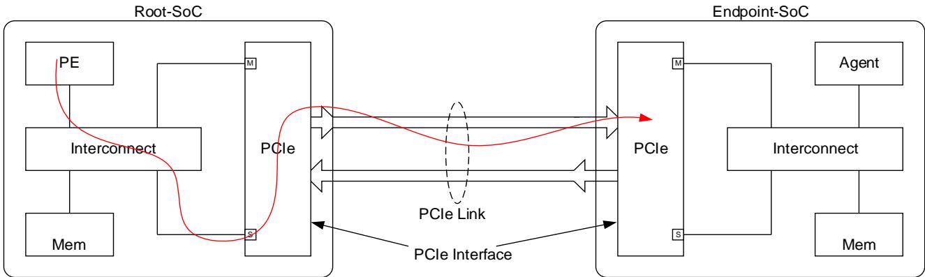
A PE generated transaction targeting a PCIe completer (an example is shown in Figure 5 below) will have ordering rules from both Arm memory model and PCIe applied to it as it flows from source to destination. This section details the end to end guarantees that the system can provide for such a transaction.
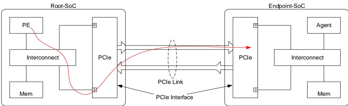
Table below shows the end to end ordering guarantee provided by the system for a PE generated PCIe transaction.
下表显示了系统为 PE 生成的 PCIe 事务提供的端到端排序保证
The table makes the following assumptions:
Software is executing on a single PE that uses the Arm memory model.
- The PE is connected via AMBA interconnect to the PCIe interface.
- All accesses are to a specific PCIe address space in a specific PCIe target.
- RO and IDO attributes are not set to 1 for transactions from the PE.
该表基于以下假设:
- 软件在单个使用 Arm 内存模型的 PE 上执行
- PE 通过 AMBA 互连连接到 PCIe 接口
- 所有访问都针对特定 PCIe 目标中的特定 PCIe 地址空间
- 来自 PE 的事务的 RO 和 IDO 属性未设置为 1
The table is read in the following way:
For each row, two accesses RW1 and RW2 from the same PE to the PCIe address space given in column 1 (e.g. configuration space), when mapped to the Arm memory type(s) given in column 2 (e.g. Device-nGnRnE) will arrive at the destination as per the ordering guarantee given in column 3 (In the example case of configuration space mapped to Device-nGnRnE, RW1 and RW2 will arrive in program order)
表的阅读方式如下:
对于每一行,来自同一 PE 的两个访问 RW1 和 RW2,当映射到第 2 列中的 Arm 内存类型时,将按第 3 列给出的排序保证到达目标
| PCIe address space | Arm memory type to which the PCIe address space is mapped | Destination arrival order guarantee provided by system to software |
|---|---|---|
| Configuration space | Device-nGnRnE (See note 1 below) | All accesses from the PE will arrive in program order. |
| Non-prefetchable memory space | Device-nGnRE or Device-nGnRnE (See note 3 below) | All accesses from the PE will arrive in program order (See note 2 below). |
| Non-prefetchable memory space | Device-nGRE | No arrival order guarantees provided by system except for accesses to the same location (See note 4 below). |
| Prefetchable memory space | Device-nGnRE or Device-nGnRnE (See note 3 below) | All accesses from the PE will arrive in program order (See note 2 below). |
| Prefetchable memory space | Normal Non-cacheable or Device-GRE or Device-nGRE | No arrival order guarantees provided by system except for accesses to the same location (See note 4, 5 and note 6 below). |
Notes:
- PCIe specification states that there must be a way for software to know that a configuration write is complete at the target [see implementation note in section 7.2.2 of [3]]. This can be achieved only by using the Device-nGnRnE memory type. Therefore, the only memory type that can be used for mapping configuration space is Device-nGnRnE.
- PCIe 规范规定必须有一种方式让软件知道配置写在目标处已完成。这只能通过使用 Device-nGnRnE 内存类型来实现。因此,唯一可用于映射配置空间的内存类型是 Device-nGnRnE。
- Program order arrival coupled with the PCIe interface enforcing PCIe ordering rules ensures that producer consumer ordering requirements are met [see section E of [4] for more details on producer consumer ordering model]. Therefore, if software requires producer consumer ordering without using barrier instructions or other ordering techniques, it must use Device-nGnRE or Device-nGnRnE.
- 程序顺序到达加上 PCIe 接口强制执行 PCIe 排序规则可确保满足生产者-消费者排序要求。因此,如果软件需要生产者-消费者排序而不使用屏障指令或其他排序技术,必须使用 Device-nGnRE 或 Device-nGnRnE。
- Writes to non-prefetchable memory space and prefetchable memory space are posted. This means that the PCIe interface will give a write completion response to the requester without getting a completion back from the target. Therefore, even if the software maps the prefetchable/non-prefetchable space as Device-nGnRnE, the completion will not come from the destination of the request. Consequently, DSB is not enough to determine that a write has reached the target for prefetchable and non-prefetchable memory spaces.
- 对不可预取内存空间和可预取内存空间的写是 posted 的。这意味着 PCIe 接口将在不从目标获取完成的情况下向请求者返回写完成响应。因此,即使软件将可预取/不可预取空间映射为 Device-nGnRnE,完成也不会来自请求的目标。DSB 不足以确定写已到达可预取和不可预取内存空间的目标。
- All accesses from a PE to the same location must arrive in program order as detailed in section 4.4.
- 如第 4.4 节所述,来自同一 PE 对同一位置的所有访问必须按程序顺序到达。
- PCIe specification permits devices to expose memory regions with read side effects as part of its prefetchable address space [see implementation note titled “Additional Guidance on the Prefetchable Bit in Memory Space BARs” in section 7.5.1.2.1 in [3]]. In such cases, software must ensure that prefetchable space with read side effects is not mapped as Normal Non-cacheable so that any unwanted side effect due to read speculation is prevented.
- PCIe 规范允许设备将具有读副作用的内存区域作为其可预取地址空间的一部分公开。在这种情况下,软件必须确保具有读副作用的可预取空间未映射为 Normal Non-cacheable,以防止因读推测而导致的任何不良副作用。
- PCIe specification permits devices to expose memory regions that cannot tolerate byte merging for writes as part of its prefetchable address space [see implementation note titled “Additional Guidance on the Prefetchable Bit in Memory Space BARs” in section 7.5.1.2.1 in [3]]. Software must ensure that prefetchable space that cannot tolerate byte merging is not mapped as Device-GRE or Normal Non-cacheable.
- PCIe 规范允许设备将不能容忍字节合并的内存区域作为其可预取地址空间的一部分公开。软件必须确保不能容忍字节合并的可预取空间未映射为 Device-GRE 或 Normal Non-cacheable。
4.8.1. Achieving producer consumer ordering for transactions from PE to PCIe destinations
As mentioned in section 4.8, the system can guarantee PCIe Producer / Consumer Ordering for Outbound PE generated PCIe transactions only if the target location(s) are mapped as Device-nGnRnE or Device-nGnRE. All other Arm memory types would require barrier instructions or other instruction ordering techniques to be used to enforce the necessary arrival order at the destination.
如第 4.8 节所述,系统仅在目标位置映射为 Device-nGnRnE 或 Device-nGnRE 时才能保证 PCIe 生产者/消费者排序。所有其他 Arm 内存类型都需要使用屏障指令或其他指令排序技术来强制执行目标处的必要到达顺序。
4.8.2. Multiple PCIe address spaces mapped as Device-nGnRnE or Device-nGnRE
Multiple PCIe address spaces mapped as Device-nGnRnE or Device-nGnRE, Arm memory model does not give any ordering guarantees between accesses to different Device-nGnRnE or Device-nGnRE peripherals. Additionally, there is no restriction on mapping various PCIe address spaces of the same PCIe function as different Device-nGnRnE or Device-nGnRE peripherals. Consequently, software cannot assume that program order will be maintained between accesses to two different PCIe address spaces, even though both spaces are mapped as Device-nGnRnE or Device-nGnRE. Therefore, for maximum software portability, ordering requirements between accesses to different PCIe address spaces must be handled explicitly in software using appropriate ordering instructions.
映射为 Device-nGnRnE 或 Device-nGnRE 的多个 PCIe 地址空间,Arm 内存模型不会对不同 Device-nGnRnE 或 Device-nGnRE 外设之间的访问提供任何排序保证。此外,将同一 PCIe 功能的多个 PCIe 地址空间映射为不同的 Device-nGnRnE 或 Device-nGnRE 外设没有限制。因此,软件不能假设即使两个空间都映射为 Device-nGnRnE 或 Device-nGnRE,两个不同 PCIe 地址空间之间的访问会保持程序顺序。因此,为了最大程度提高软件可移植性,必须在软件中显式处理不同 PCIe 地址空间之间访问的排序要求,使用适当的排序指令。
5. COMPLYING TO PCIE ORDERING MODEL
PCle ordering requirements are specified in the form of an ordering rules table in the PCIe specification [see section 2.4 in [3]]. The primary purpose of the PCIe ordering model is to achieve producer-consumer ordering and to avoid deadlock. This section details the requirements that the PCIe interface in a Root-SoC or Endpoint-SoC must meet for complying with PCIe ordering model.
PCIe 排序要求以 PCIe 规范中的排序规则表形式指定 [见第 2.4 节]。PCIe 排序模型的主要目的是实现生产者-消费者排序并避免死锁。本节详细说明了 Root-SoC 或 Endpoint-SoC 中的 PCIe 接口为符合 PCIe 排序模型必须满足的要求。
The organization of rest of this section is as follows:
本节其余部分的组织如下:
In section 5.1, the rules in the table are discussed in brief and the coverage of the rules in this document is listed.
在第 5.1 节中,将简要讨论表中的规则,并列出本文档对这些规则的覆盖范围。
In section 5.2, the table is broken down in terms of the rules for Ordering and Overtaking. Ordering rules describe when requests and completions must be kept in the order in which they were received by the PCIe interface to ensure that producer consumer ordering model is not violated. The Overtaking rules describe when certain requests or completions must be able to pass other requests or completions that are blocked to avoid deadlock.
在第 5.2 节中,将表分解为排序 (Ordering) 和超越 (Overtaking) 规则。排序规则描述了请求和完成必须按照 PCIe 接口接收的顺序保持的时机,以确保不违反生产者-消费者排序模型。超越规则描述了某些请求或完成必须能够通过其他被阻塞的请求或完成以避免死锁的时机。
In section 5.3, the requirements for complying with the overtaking rules identified in section 5.2 are discussed in detail.
在第 5.3 节中,将详细讨论为符合第 5.2 节中确定的超越规则而满足的要求。
In section 5.4, the requirements for complying with the ordering rules identified in section 5.2 are discussed in detail.
在第 5.4 节中,将详细讨论为符合第 5.2 节中确定的排序规则而满足的要求。
Note: Unless explicitly stated, a given requirement must be met by the PCIe interface in both Root-SoC and Endpoint-SoC.
5.1. Ordering table coverage
PCle ordering rules are given in the table below [as per section 2.4 in [3]].
PCIe 排序规则如下表所示 [根据第 2.4 节]。
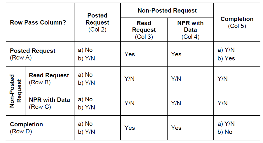
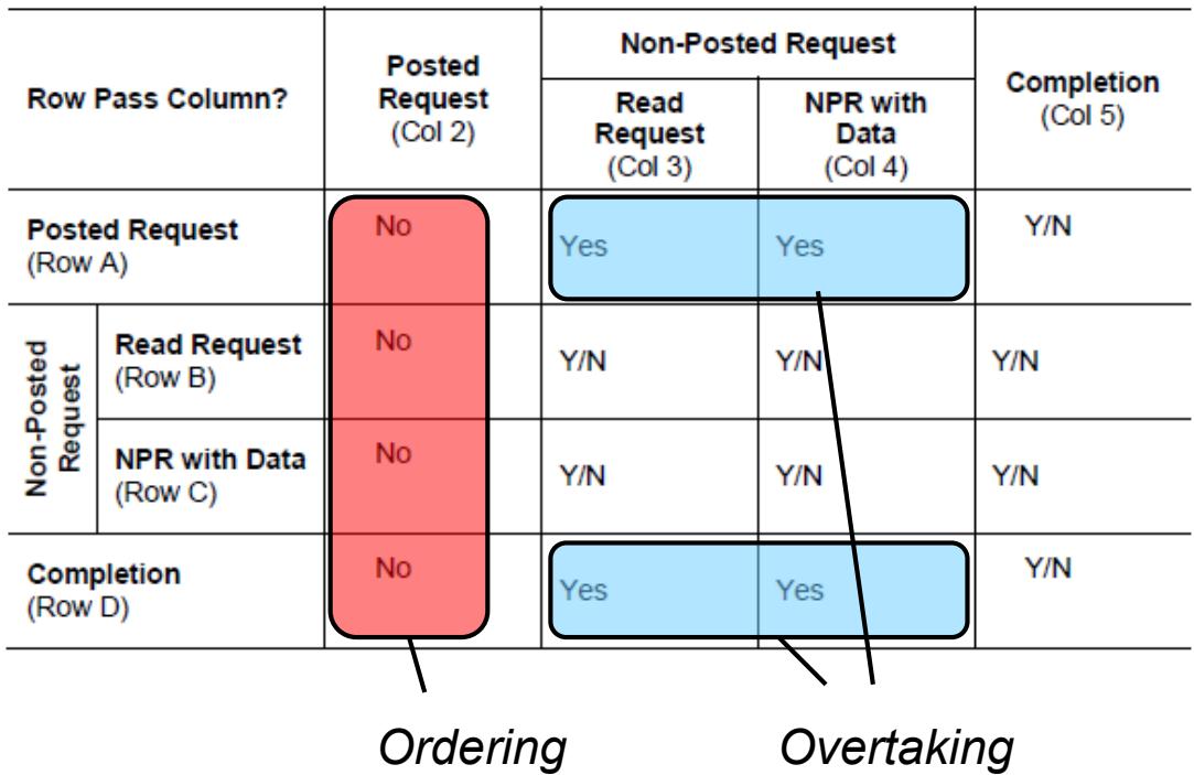
Entries A2b, B2b, C2b and D2b do not need to be considered for functional correctness. These entries all permit one request to pass another when certain conditions (such as RO and/or IDO permit). The system is always functionally correct if the ability for one request to pass another is ignored, but it may be lower performance. Once it has been established that a system is completely functionally correct, the relaxations permitted by these entries can be used to improve performance. This document covers the requirements for correct implementation of functional correctness rules (A2a, B2a, C2a, D2a) and performance enhancement rules (A2b, B2b, C2b, D2b).
条目 A2b、B2b、C2b 和 D2b 不需要考虑功能正确性。这些条目都允许在满足某些条件(如 RO 和/或 IDO 允许)时一个请求通过另一个请求。如果忽略一个请求通过另一个请求的能力,系统在功能上始终是正确的,但性能可能会降低。一旦确定系统在功能上完全正确,就可以利用这些条目允许的放宽来提高性能。本文档涵盖正确实施功能正确性规则(A2a、B2a、C2a、D2a)和性能增强规则(A2b、B2b、C2b、D2b)的要求。
Note: It is worth noting that the relaxations permitted by these entries are not symmetric.
注意:值得注意的是,这些条目允许的放宽是不对称的。
- Posted requests do not overtake posted requests. Except for RO or IDO. (Rule A2b)
- Read requests do not overtake posted requests. Except for IDO. (Rule B2b)
- Non-posted request do not overtake posted requests. Except for RO or IDO. (Rule C2b)
- Read completions do not overtake posted requests. Except for RO or IDO. (Rule D2b)
- Posted 请求不会超越 Posted 请求。除 RO 或 IDO 外。(规则 A2b)
- 读请求不会超越 Posted 请求。除 IDO 外。(规则 B2b)
- Non-posted 请求不会超越 Posted 请求。除 RO 或 IDO 外。(规则 C2b)
- 读完成不会超越 Posted 请求。除 RO 或 IDO 外。(规则 D2b)
Note that RO relaxation does not apply to “Read requests do not overtake posted requests”.
注意:RO 放宽不适用于"读请求不会超越 Posted 请求"。
Entry D2b also permits a configuration write completion to pass a posted request in all cases.
条目 D2b 还允许配置写完成在所有情况下超越 Posted 请求。
Entry A5b relates only to PCI/PCl-X bridges. Therefore, this rule is not relevant and is not covered in this document.
Entry D5b requires that completions with the same Transaction ID must not pass. It does not add extra requirements between the completions of different transactions. Therefore, this rule is not discussed further in this document.
All other entries that are “Y/N” in the table need not be considered for functional correctness with respect to the PCIe ordering model. Hence, they do not impose any additional PCIe ordering related requirements on the PCIe interface and are not discussed further in this section.
表中所有其他“Y/N”条目无需考虑 PCIe 排序模型的功能正确性。
The table below summarizes the rules coverage in this document:
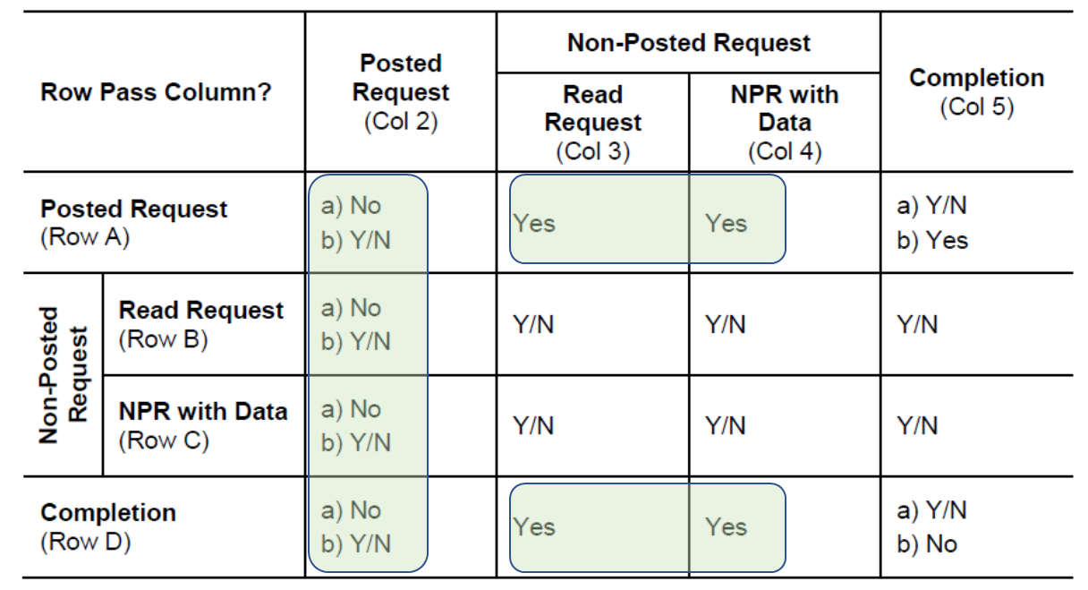
All entries within the green boxes are covered in this document.
5.2. Overtaking and Ordering
There are two ways to categorize the entries in the table. Firstly, whether they are ordering rules, where order must be maintained, or overtaking rules, where one transaction must be able to pass another to avoid deadlock if the earlier transaction is blocked. This categorization is shown in the table below. Note that the performance optimization related rules (A2b, B2b, C2b, D2b) are not shown in the table.
对表中的条目进行分类有两种方式。
- 是排序规则,即必须保持顺序(Order);
- 是超车(Overtaking)规则,即如果较早的事务被阻塞,一个事务必须能够通过另一个事务以避免死锁
For a PCIe interface, the overtaking and ordering rules must be applied for the following:
- Requests and completions that are coming into the PCIe interface from the link.
- Requests and completions that the PCIe interface is sending out.
对于 PCIe 接口,必须对以下情况应用 Overtaking 和 Order 规则:
- 从链路进入 PCIe 接口的请求和完成。
- PCIe 接口正在发送出去的请求和完成。
Outbound and Inbound Traffic on the PCIe link for the PCIe interface in a Root-SoC and that of an Endpoint-SoC is shown in Figure.
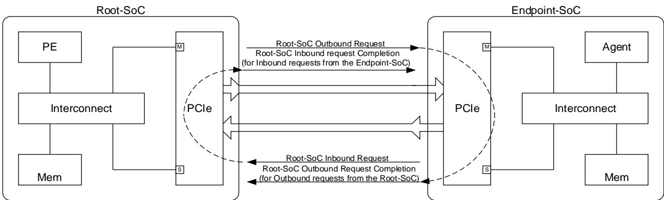
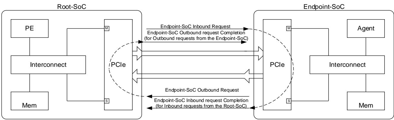
Table below highlights the rules that apply between two requests and rules that apply between a completion and a request.
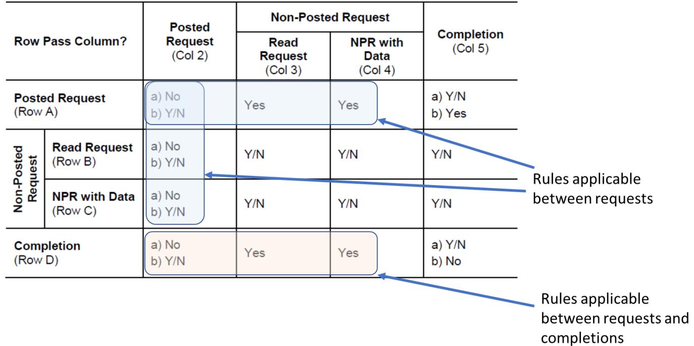
From this table, it is evident that the overtaking and ordering requirements must be considered for the following cases:
- Both requests Outbound
- Both requests Inbound
- Outbound request / Inbound completion
- Outbound completion/ Inbound request
For Overtaking rules, “Both requests Outbound” and “Both requests Inbound” consider the overtaking rules of multiple requests, as described in table cells A3 and A4. While “Outbound request / Inbound completion” and “Outbound completion/ Inbound request” consider the overtaking rules between requests and completions, as described in table cells D3 and D4.
对于 Overtaking 规则,“两个请求出站”和“两个请求入站”考虑了多个请求的 Overtaking 规则,如表单元格 A3 和 A4 所述。而“出站请求/入站完成”和“出站完成/入站请求”考虑了请求和完成之间的超车规则,如表单元格 D3 和 D4 所述。
For Ordering rules, “Both requests Outbound” and “Both requests Inbound” consider the ordering rules of multiple requests, as described in table cells A2, B2 and C2. While “Outbound request / Inbound completion” and “Outbound completion/ Inbound request” consider the ordering rules between requests and completions, as described in table cell D2.
对于排序规则,“两个请求出站”和“两个请求入站”考虑了多个请求的排序规则,如表单元格 A2、B2 和 C2 所述。而“出站请求/入站完成”和“出站完成/入站请求”考虑了请求和完成之间的排序规则,如表单元格 D2 所述。
5.3. Overtaking Rules
This section considers the overtaking rules. These rules are all based on the principle that any packet which does not require a packet to flow in the opposite direction should make forward progress. So, read transaction completions (which are the last stage of a read transaction) are required to make forward progress and posted write transactions (which only require packets in one direction) are required to make forward progress.
任何不需要数据反向流动的包都应该向前推进。因此,读事务完成(读事务的最后阶段)需要向前推进,而 Posted 写事务(只需要单向数据包)也需要向前推进。
5.3.1. Both requests Outbound
出站请求
This describes the overtaking rules that apply for two Outbound requests being received by the PCIe Interface Subordinate port.
5.3.1.1. Posted Write must be able to overtake Read Request [A3]
Posted 写必须越过读请求
A PCIe Interface must ensure that an Outbound posted write received from the AMBA interconnect is able to overtake blocked Outbound read requests even though the read requests were received earlier than the posted write.
For peer-to-peer traffic in a Root-SoC, it is required that there is a non-blocking path for Inbound posted writes coming into one PCIe interface to go out as Outbound posted writes in another PCIe interface through the AMBA interconnect. This non-blocking path must not use any shared read/write resource, to avoid read backpressure blocking the posted writes.
PCIe 接口必须确保从 AMBA 互连接收到的出站 Posted 写请求能够超越被阻塞的出站读请求,即使这些读请求比 Posted 写请求更早接收。
对于 Root-SoC 中的 Peer-to-Peer 流量,要求从一个 PCIe 接口进入的入站 Posted 写能够通过 AMBA 互连作为出站 Posted 写从另一个 PCIe 接口出去,并且这条路径必须是非阻塞的。这条非阻塞路径不得使用任何共享读/写资源,以避免读反压阻塞 Posted 写。
5.3.1.2. Posted Write must be able to overtake Configuration Write [A4]
Posted 写必须能够超越 Configuration 写
A PCIe Interface must ensure that an Outbound posted write received from the AMBA interconnect is able to overtake blocked Outbound configuration write requests even though the configuration write requests were received earlier than the posted write.
PCIe 接口必须确保从 AMBA 互连接收到的出站 Posted 写能够超越被阻塞的出站 Configuration 写请求,即使 Configuration 写请求比 Posted 写更早接收。
It is strongly recommended that a PCIe Interface can accept at least one configuration write, whilst still allowing subsequent posted writes to be accepted and be able to overtake the configuration write. To implement this requirement consideration needs to be given to configuration writes and posted writes that use the same AXI ID, as the AXI write responses must be given in the same order that the requests are received.
强烈建议 PCIe 接口至少能够接受一个 Configuration 写,同时仍然允许后续的 Posted 写被接受并能够超越 Configuration 写。为了实现此要求,需要考虑使用相同 AXI ID 的 Configuration 写和 Posted 写,因为 AXI 写响应必须按照请求接收的相同顺序给出。
The AMBA system must ensure there is no back pressure on Inbound requests. It must ensure that any back pressure on configuration writes or posted writes does not block the progress of snoop transactions for Inbound requests. See section 6.2 for further details.
AMBA 系统必须确保入站请求没有反压。它必须确保 Configuration 写或 Posted 写上的任何反压不会阻塞入站请求的 Snoop 事务的进展。有关详细信息,请参见 6.2. IO Coherent PCIe Traffic。
In a system where it is possible for multiple configuration writes to happen concurrently, the PCIe Interface must be capable of accepting all configuration writes that are presented to it, whilst still allowing subsequent posted writes to be accepted and to overtake the configuration writes.
在可能同时发生多个 Configuration 写的系统中,PCIe 接口必须能够接受所有呈现给它的 Configuration 写,同时仍然允许后续的 Posted 写被接受并超越 Configuration 写。
5.3.2. Both requests Inbound
入站请求
This describes the overtaking requirements that apply for two Inbound requests being issued by the PCIe Interface Manager port.
5.3.2.1. Posted Write must be able to overtake Read Request [A3]
Posted 写必须能够超越读请求
A PCIe Interface must ensure that an Inbound posted write request is able to overtake Inbound read requests. This requires that the PCIe Interface can issue a write request into the AMBA interconnect even if read requests that were received earlier are yet to be issued into the AMBA interconnect. This ensures that even if the read channel of the AMBA interconnect is blocked, Inbound posted writes can make forward progress.
PCIe 接口必须确保入站 Posted 写请求能够超越入站读请求。这要求 PCIe 接口能够将写请求发往 AMBA 互连,即使较早接收的读请求尚未发往 AMBA 互连。这确保了即使 AMBA 互连的读取通道被阻塞,入站 Posted 写也能够向前推进。
Note that the PCIe interface must guarantee that it can always accept the data returned by the AMBA interconnect for a read request it has made. In practice, this means that the PCIe interface must not issue a read request into the AMBA interconnect unless it has buffer space reserved for the read data.
请注意,PCIe 接口必须保证它总是能够接受 AMBA 互连为其已发出的读请求返回的数据。在实践中,这意味着 PCIe 接口不得向 AMBA 互连发出读请求,除非它已为读取数据预留了缓冲空间。
For peer-to-peer traffic in a Root-SoC, the same requirement for a non-blocking path from Inbound posted writes to Outbound posted writes in the AMBA system exists, as described above.
对于 Root-SoC 中的 peer-to-peer 流量,如上所述,AMBA 系统中同样存在从入站 Posted 写到出站 Posted 写的非阻塞路径的要求。
5.3.2.2. Posted Write must be able to overtake Configuration Write [A4]
Posted 写必须能够超越 Configuration 写
This rule has different implications in a Root-SoC PCIe interface versus in an Endpoint-SoC PCIe interface.
5.3.2.2.1. For the Root-SoC PCIe interface
Inbound configuration writes are not supported for Root-SoC devices. This also means that there are no implications for peer-to-peer traffic.
Root-SoC 设备不支持入站 Configuration 写。这也意味着对 peer-to-peer 流量没有影响。
5.3.2.2.2. For the Endpoint-SoC PCIe interface
An Inbound configuration write to an Endpoint-SoC is generally not expected to propagate past the PCIe Interface.
However, if the configuration write does propagate past the PCIe interface, then the PCIe Interface must ensure that an Inbound configuration write cannot block an Inbound posted write request.
This requires that the PCIe Interface must be able to perform the following:
The PCIe Interface can issue a write request into the AMBA interconnect even if Configuration write requests that were received earlier are yet to be issued into the AMBA interconnect. The PCIe interface can issue a later posted write request before the earlier configuration write request completion is returned on the PCIe link.
For the case where Inbound configuration write is sunk within the PCIe interface, the PCIe interface must ensure that Inbound posted write can be issued into the AMBA interconnect even if there are Inbound Configuration writes received earlier waiting to be sunk by the PCIe interface.
通常情况下,发往 Endpoint-SoC 的入站配置写不应传播到 PCIe 接口之外。
但是,如果 Configuration 写确实传播到了 PCIe 接口之外,那么 PCIe 接口必须确保入站 Configuration 写不能阻塞入站 Posted 写请求。
这要求 PCIe 接口必须能够执行以下操作:
PCIe 接口能够将写请求发往 AMBA 互连,即使较早接收的 Configuration 写请求尚未发往 AMBA 互连。PCIe 接口可以在较早的 Configuration 写请求的完成在 PCIe 链路上返回之前,发出一个较晚的 Posted 写请求。
对于入站 Configuration 写在 PCIe 接口内部被吸收(sunk)的情况,PCIe 接口必须确保,即使有较早接收的、正在等待被 PCIe 接口吸收的入站 Configuration 写,入站 Posted 写也能够被发往 AMBA 互连。
5.3.3. Outbound request / Inbound Completion
出站请求 / 入站完成
This describes the overtaking requirements of two packets, one is an Outbound request that is being received by the PCIe Interface Subordinate port and the other is an Inbound completion returning via the PCIe Interface Manager port.
- PCIe 接口 PCIe Interface Subordinate port 接收的出站请求
- PCIe Interface Manager port 返回的入站完成。
5.3.3.1. Inbound completion must be able to overtake Outbound Read Request or Configuration Write. [D3, D4]
入站完成必须能够超越出站读请求或配置写
A PCIe Interface must ensure that completions for Inbound read requests (termed as “Inbound Completions”) are not blocked by Outbound read requests or configuration write requests. This means that the PCIe interface can schedule completions for Inbound read requests ahead of Outbound requests and Outbound configuration write requests that are blocked (e.g. due to lack of appropriate flow control credits).
PCIe 接口必须确保入站读请求的完成(称为“入站完成”)不会被出站读请求或 Configuration 写请求阻塞。这意味着 PCIe 接口可以将入站读请求的完成调度在被阻塞的出站读请求和出站 Configuration 写请求之前(例如,由于缺乏适当的流控制信用)。
PCIe Interface must also ensure that the need for Inbound completions to not overtake Outbound posted writes, does not prevent Inbound completions from overtaking Outbound read requests or configuration write requests.
PCIe 接口还必须确保,入站完成不得超越出站 Posted 写。
There is no implication in the AXI or ACE interconnect domain, as read data (which eventually becomes the completion for the Inbound read request) is always returned without requiring forward progress on requests flowing in the same direction.
在 AXI 或 ACE 互连中没有影响,因为读取数据(最终成为入站读请求的完成)总是返回,而不需要同方向流动的请求向前推进。
5.3.4. Outbound completion/ Inbound request
出站完成 / 入站请求
This describes the overtaking requirements of two packets, one is an Inbound request being issued by the PCIe Interface Manager port and the other is an Outbound completion (for an Outbound request transaction) returning via the PCIe Interface Subordinate port.
- PCIe Interface Manager port 发出的入站请求
- PCIe Interface Subordinate port 返回的出站完成(针对出站请求事务)。
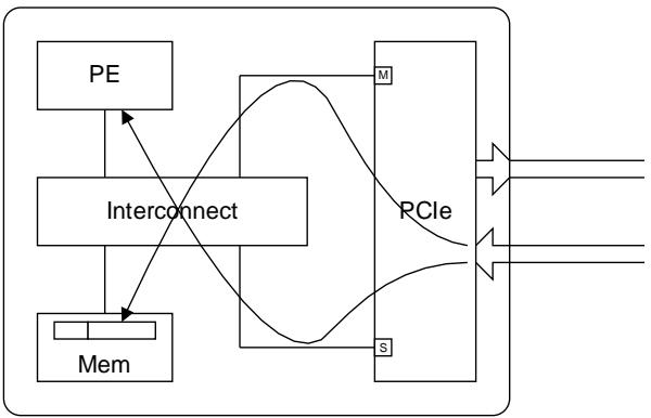
5.3.4.1. Outbound Completion must be able to overtake Inbound Read Request or Configuration Write. [D3, D4]
出站完成必须能够超越入站读请求或配置写。
A PCIe Interface must ensure that completions for Outbound read requests and Outbound configuration write requests (termed as “Outbound completion”) are not blocked by Inbound read requests or Configuration write requests. This means that the PCIe interface is able to let Outbound completions reach the AMBA interconnect ahead of Inbound read requests and Inbound configuration write requests which are blocked from being sent into the AMBA interconnect (e.g. read requests being blocked due to the AMBA read channel being not ready).
PCIe 接口必须确保出站读请求和出站 Configuration 写请求的完成(称为“出站完成”)不会被入站读请求或 Configuration 写请求阻塞。这意味着 PCIe 接口能够让出站完成在入站读请求和入站 Configuration 写请求被阻塞而无法发送到 AMBA 互连(例如,读请求由于 AMBA 读取通道未就绪而被阻塞)之前到达 AMBA 互连。
PCIe Interface must also ensure that the need for Outbound completions to not overtake Inbound posted writes, does not prevent Outbound completions from overtaking Inbound read requests or configuration write requests.
PCIe 接口还必须确保,出站完成不得超越入站 Posted 写,不会阻止出站完成超越入站读请求或 Configuration 写请求。
There is no implication in the AXI or ACE interconnect domain, as read data or write response from an Outbound completion can flow through the interconnect without requiring forward progress of requests flowing in the same direction.
在 AXI 或 ACE 互连域中没有影响,因为来自出站完成的读数据或写入响应可以流经互连网络,而不需要同方向流动的请求向前推进。
5.4. Ordering Rules
This section considers the ordering rules required to maintain the PCIe producer-consumer ordering model.
Each sub-section starts with a diagrammatic overview of the case being considered, followed by a summary of the requirements and then finally a use case example is given.
The use cases examples are intended to clarify the reasoning behind certain ordering requirements, but they do not form part of the requirements or attempt to describe every aspect that needs to be considered.
Note: In the many of the use case examples the Endpoint is considered as being a simple UART like device, with register access to features such as a write-only transmit buffer, a read-only receive buffer, a writeable register to force the transmit buffer to flush and a readable buffer status register to indicate the number of entries in both transmit/receive buffers. Whilst this simple example is not realistic, it is useful to illustrate why the ordering of two accesses to registers at different memory location may require to be ordered.
5.4.1. Both requests Outbound
This describes the ordering requirements of two packets that are both Outbound requests being received by the PCIe Interface Subordinate port.
出站 (Outbound): 指的是请求从系统内部(即 CPU 核心或内存)发起,通过 PCIe 接口发送到外部的 PCIe 设备。
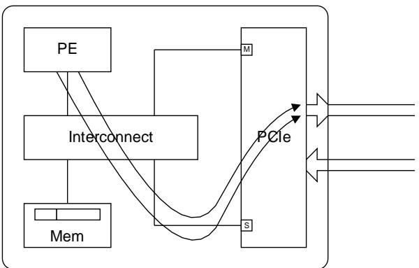
5.4.2. Posted Write, Read Request, or Configuration Write must not overtake Posted Write [A2, B2, C2]
Posted Write、Read Request 或 Configuration Write 不得越过 Posted Write
For complying with this ordering requirement, the PCIe interface requirements are as follows:
For Outbound posted writes with RO = 0 and IDO = 0 , Outbound Read requests with IDO = 0 and Outbound Configuration writes with IDO = 0 [A2a, B2a, C2a in the PCIe ordering table]: ^a66d7e
- Outbound read requests, posted write requests and configuration write requests must not be allowed to overtake an earlier Outbound posted write for which a completion response has been returned to the AMBA interconnect.
对于严格排序的情况 (
RO=0,IDO=0),出站的读请求、Posted 写请求和 Configuration 写请求,不得越过一个更早发出的、尚未收到完成响应的出站 Posted 写请求。
For posted writes with RO = 1 and IDO = 0 or RO = 1 and IDO = 1 [A2b in the PCIe ordering table]:
- Outbound posted writes with
RO = 1can overtake earlier Outbound posted writes for which a completion response has been returned to the AMBA interconnect. Note that value of IDO need not be considered whenRO = 1.
对于启用宽松排序的 Posted 写 (
RO=1),当一个出站 Posted 写请求的RO位被设置为 1 时,它可以越过一个更早发出的、但尚未收到完成响应的出站 Posted 写请求。
For posted writes with RO = 0 and IDO = 1 [A2b in the PCIe ordering table]:
- Outbound posted writes with
RO = 0andIDO = 1can overtake earlier Outbound posted writes for which a completion response has been returned to the AMBA interconnect provided either of the following are true:- Requester ID of the two writes are different
- Both writes have PASID prefixes (relevant only for Endpoint-SoC), and the PASID values are different.
一个属性为
RO=0和IDO=1的出站 Posted 写请求,可以越过一个更早发出的出站 Posted 写请求,前提是满足以下任一条件:
- 两个写请求的 Requester ID 不同。Requester ID: 在 PCIe 中,每个可以发起请求的设备功能(Function)都有一个唯一的 ID(由总线号、设备号、功能号组成),这个 ID 标识了请求的来源。如果两个写请求来自不同的源头(例如,一个来自 CPU,另一个来自 DMA 控制器),系统就认为它们是相互独立的,允许后发的请求先于先发的请求完成,因为它们不太可能操作相关联的数据。
- 两个写请求都有 PASID 前缀,且 PASID 值不同。PASID (Process Address Space ID, 进程地址空间 ID): 这是一个用于虚拟化环境的特性。它允许一个物理设备(如一个 PCIe 网卡)同时被多个虚拟机(VM)或进程使用。PASID 用于区分这个请求是属于哪个 VM 或进程的。即使两个写请求发往同一个物理设备,但如果它们属于不同的虚拟机(即 PASID 不同),系统也认为它们是独立的,因而允许乱序执行。
For Read requests with IDO = 1 [B2b in the PCIe ordering table]:
- Outbound Read requests with
IDO = 1can overtake earlier Outbound posted writes for which a completion response has been returned to the AMBA interconnect provided either of the following is true:- Requester IDs of write and the read are different.
- Both write request and read request has PASID prefix (relevant only for Endpoint-SoC), and the PASID values are different.
一个属性为
IDO=1的出站读请求,可以越过一个更早发出的出站 Posted 写请求,前提是满足以下任一条件:
- 写请求和读请求的 Requester ID 不同。如果一个设备(如 DMA)正在向内存写入数据,而另一个设备(如 CPU)需要从一个完全无关的内存区域读取数据,那么没有必要让读取操作等待写入操作完成。
- 写请求和读请求都有 PASID 前缀,且 PASID 值不同。如果虚拟机 A 的读请求和虚拟机 B 的写请求都发往同一个共享设备,只要这两个请求是相互独立的(通过不同的 PASID 来标识),读取就可以越过写入。
For Configuration write requests with RO = 1 or IDO = 1 [C2b in the PCIe ordering table]:
- Outbound configuration write requests with (
RO = 1andIDO = 0) or (RO = 1andIDO = 1) can overtake earlier Outbound posted writes for which a completion response has been returned to the AMBA interconnect provided the following is true:- Requester IDs of the posted write and configuration write are different.
- Outbound configuration write requests with (
RO = 1andIDO = 0) or (RO = 1andIDO = 1) can overtake earlier Outbound posted writes for which a completion response has been returned to the AMBA interconnect. Note that value of IDO need not be considered whenRO = 1
对于 Configuration 写请求 (
RO=1或IDO=1)
RO=0和IDO=1: 一个属性为RO=0和IDO=1的出站 Configuration 写请求,可以越过一个更早发出的出站 Posted 写请求,前提是它们的 Requester ID 不同。Configuration 写通常用于设置或修改设备的配置寄存器。如果这个 Configuration 写请求和另一个数据写请求来自不同的源头,它们可以乱序执行。RO=1: 一个属性为RO=1的出站 Configuration 写请求,可以越过一个更早发出的出站 Posted 写请求。RO=1(宽松排序)是一个比IDO=1更强的“放行”信号。一旦一个事务被标记为宽松排序 (RO=1),它就被赋予了最大的乱序自由度,可以越过它前面的(某些类型的)未完成事务,而无需再检查它们的 ID 是否相同。
5.4.2.1. Example Use Cases
5.4.2.1.1. Usage model example for rule A2a
An example usage that requires multiple Outbound posted writes to be kept in the order in which the requester intended them to reach the completer would be a series of writes to data buffer followed by a write to valid flag location which indicates that the data is available. If ordering was not maintained, then it would be possible for the valid flag to be observed by the endpoint before all the data buffer writes had occurred. See A2a.
A2a 规则强制所有这些 Posted 写必须按序到达。设备只有在收到了所有数据块之后,才会收到最后的“标志位”写入。这就保证了数据处理的正确性。
5.4.2.1.2. Usage model example for rule B2a
An example usage model that requires Outbound reads to be prevented from overtaking Outbound posted writes is the following sequence:
- Endpoint A sends a peer to peer write to Endpoint B via the Root-SoC.
- Endpoint A writes a flag in Root-SoC memory indicating that the data is ready in Endpoint B’s buffer.
- Software reads the flag as set and sends a read to get the data from Endpoint B.
- Both the software read from Endpoint B and Endpoint A write to Endpoint B goes out through the same PCIe interface.
- This means that if software read of the buffer in Endpoint B overtakes Endpoint A’s write to the same buffer, then software would get stale data. Therefore, it is necessary that Outbound reads do not overtake Outbound posted writes in this usage model.
- Endpoint A 通过 Root-SoC 向 Endpoint B 发送一个 peer to peer 写操作。
- Endpoint A 在 Root-SoC 的内存中写入一个标志位,用以表明 Endpoint B 缓冲区中的数据已准备就绪。
- Software 读取该标志位,确认其被置位后,便发送一个读请求,以从 Endpoint B 获取数据。
- 软件对 Endpoint B 的读请求和 Endpoint A 对 Endpoint B 的写操作,均通过同一个 PCIe 接口发出。
- 这意味着,如果对 Endpoint B 缓冲区的读请求,超越了 Endpoint A 对同一缓冲区的写操作,那么软件就会获取到陈旧(stale)的数据。因此,在该使用场景中,必须确保 Outbound 读取不会超越 Outbound Posted 写。
See B2a.
B2a 规则禁止读请求越过写请求。它确保了软件的读取操作必须等待 Endpoint A 的写入操作完成后才能执行,从而保证软件能读到最新的数据。
5.4.2.1.3. Usage model example for rule C2a
An example usage model that requires Outbound configuration writes to be prevented from overtaking Outbound posted write is the following sequence:
- Software writes data to Endpoint A’s memory space using posted writes.
- Software writes to a configuration register in Endpoint A to trigger usage of the data written in (1).
- This means that if configuration write overtakes posted writes, then stale data would be used. Therefore, it is necessary that Outbound configuration writes do not overtake Outbound posted writes in this usage model.
- Software 使用 posted 写操作将数据写入 Endpoint A 的内存空间。
- Software 向 Endpoint A 的一个配置寄存器(configuration register)写入信息,以触发对步骤 (1) 中所写入数据的使用。
- 这意味着,如果对配置寄存器的写操作超越了之前的 posted 写操作,那么 Endpoint A 将会使用到陈旧(stale)的数据。因此,在该使用场景中,必须确保 Outbound configuration 写操作不会超越 Outbound posted 写操作。
See C2a.
C2a 规则强制 Configuration 写必须等待在它前面的 Posted 写完成。这确保了“触发”命令总是在数据完全准备好之后才被设备接收和执行。
5.4.3. Both requests Inbound
This describes the ordering requirements of two packets that are both Inbound requests being issued by the PCIe Interface Manager port.
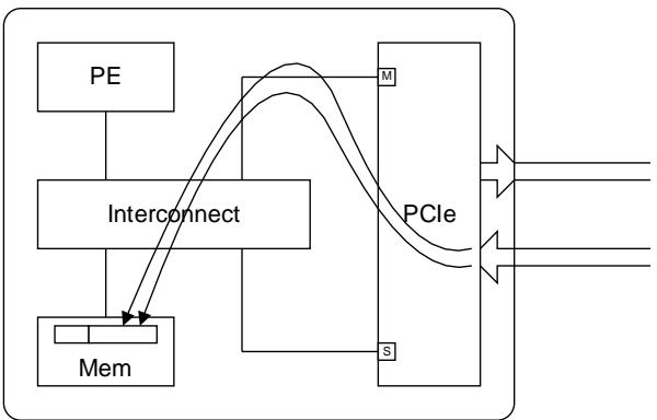
入站 (Inbound): 指的是外部的 PCIe 设备通过 PCIe 接口发送到系统内部(例如内存)。
5.4.3.1. Posted Write must not overtake Posted Write [A2]
Posted Write 不得越过 Posted Write
A PCIe Interface must maintain write ordering required for the PCIe ordering model by the appropriate use of AXI IDs for write requests and the serialization of write requests.
PCIe 接口必须通过正确使用 AXI ID 和序列化写请求,来维持 PCIe 模型所要求的写入顺序
The exact ordering requirements of between two Inbound write requests will depend on the RO and IDO attributes of the requests as detailed below:
取决于入站写请求的
RO和IDO属性
5.4.3.1.1. Inbound posted write with IDO = 0 and RO = 0 [Rule A2a in the PCIe ordering table]
In this case, all observers in the system must observe Inbound posted writes in the order in which they were received from the link by the PCIe interface. To guarantee the required ordering of an Inbound posted write with Inbound posted writes that arrived earlier, the PCIe interface can do one of the following:
- It issues the posted write request into the AMBA interconnect only after a completion response has been received for all earlier write requests.
- It issues posted writes into the AMBA interconnect in a pipelined manner by doing one of the following:
- It uses the Ordered_Write_Observation property. The Ordered_Write_Observation property defines that the interface will ensure that all requests with the same AXI ID will be observed in the order in which they were issued into AMBA interconnect by the PCIe interface. Typically, this is supported by the interconnect scheduling the requests and using its knowledge of the system address map to ensure two requests are not issued in a pipelined manner if they are to different peripherals.
- It takes advantage of the fact that all transactions to the same peripheral with the same AXI ID will be observed in the order in which they were issued into AMBA interconnect by the PCIe interface. This is done when the interface knows that all outstanding writes (i.e. previously issued writes for which completion response has not been received from the AMBA interconnect yet) are to the same peripheral. Note that when issuing a request to a different peripheral it is necessary to wait till all earlier write requests have received their completion response.
To take advantage of these two methods, a posted write with IDO = 0 and RO = 0 must be issued with the AXI ID of outstanding writes (i.e. previously issued writes for which completion response has not been received from the AMBA interconnect yet) that had IDO = 0 and RO = 0 .
Note that posted write with a certain AXI ID can be issued into the AMBA interconnect only after completion response has been received for all previously issued writes with a different AXI ID.
Inbound posted write (
IDO=0,RO=0)系统中的所有 observers 都必须按照 PCIe 接口从 link 接收的顺序,来观察到 Inbound posted 写的发生。为保证一个 Inbound posted write 与其之前到达的 Inbound posted write 之间满足所需的顺序
串行方式:仅当收到所有先前写请求的完成响应后,才将该 Posted 写发往 AMBA 互连总线。
流水线方式:通过采用以下方法之一,以流水线(pipelined)方式将 Posted 写发往 AMBA 互连总线:
- 使用
Ordered_Write_Observation属性。该属性定义了接口需确保:所有具有相同 AXI ID 的请求,都将按照它们被 PCIe 接口发往 AMBA 互连总线的顺序被观察到。通常,这一特性由互连总线提供支持,它会调度这些请求,并利用其对系统地址映射(system address map)的认知,来确保发往不同外设(peripherals)的两个请求不会以流水线方式被发出。- 利用对同一外设的有序性。此方法利用了以下事实:所有发往同一外设且具有相同 AXI ID 的事务,都将按照它们被 PCIe 接口发往 AMBA 互连总线的顺序被观察到。当接口获知所有未完成的(outstanding)写操作(即,已发出但尚未从 AMBA 互连总线收到完成响应的写操作)都是发往同一外设时,便可采用此方法。请注意,当需要向一个不同的外设发出请求时,则必须等待所有先前的写请求都收到其完成响应。
5.4.3.1.2. Inbound posted write with IDO = 1 and RO = 0 [Rule A2b in the PCIe ordering table]
For Inbound posted writes with IDO = 1 and RO = 0, the PCIe interface can do one of the following:
- It issues posted writes into the AMBA interconnect in a pipelined manner by doing one of the following:
- It uses the Ordered_Write_Observation property.
- It takes advantage of the fact that all transactions to the same peripheral with the same AXI ID will be observed in the order in which they were issued into AMBA interconnect.
To take advantage of these two methods, a posted write with a certain PCIe Requester ID or PASID must be issued with the AXI ID of outstanding writes that had the same PCIe Requester ID or PASID.
Each PCIe Requester ID and each PASID is expected have its own unique AXI ID for posted writes. This ensures that all posted writes with same PCIe Requester ID or the same PASID remains in the order in which they were received from the link while allowing re-ordering between posted writes having different PCIe Requester IDs or different PASIDs.
Note that a posted write having IDO = 1 and RO = 0 can be issued into the AMBA interconnect with a certain AXI ID only if the following conditions are true:
- All previously issued writes that had the same PCIe Requester ID but a different AXI ID has received their completion response.
- If the posted write has PASID prefix, then all previously issued writes that had the same PASID but a different AXI ID has received their completion response.
- It ignores the
IDO = 1setting and uses one of the options listed in the section titled Inbound posted write withIDO = 0andRO = 0[Rule A2a in the PCIe ordering table] while issuing the posted write into the AMBA interconnect.
Inbound posted writes (
IDO=1,RO=0)对于
IDO = 1且RO = 0的入站 Inbound posted 写操作,PCIe 接口可以执行以下操作之一:
- 利用 ID 维持顺序:它以流水线的方式将 posted 写操作发往 AMBA 互连总线,具体方法为以下二者之一:
- 利用
Ordered_Write_Observation属性。- 利用以下事实:所有发往同一外设且具有相同 AXI ID 的事务,其被观测到的顺序将与它们被发往 AMBA 互连时的顺序保持一致。
- 为了利用这两种方法,一个带有特定 PCIe Requester ID 或 PASID 的 Posted 写操作,必须使用与之前已发出(但尚未完成)的、且具有相同 PCIe Requester ID 或 PASID 的写操作所使用的相同 AXI ID。
- 设计上要求为每个 PCIe Requester ID 和每个 PASID 分配其专属的、用于 Posted 写操作的唯一 AXI ID。这可以确保:所有具有相同 PCIe Requester ID 或相同 PASID 的 Posted 写操作,能够保持其从 PCIe 链路接收时的顺序;与此同时,允许在具有不同 PCIe Requester ID 或不同 PASID 的 Posted 写操作之间进行重排序(和
IDO = 0andRO = 0区别)。- 请注意,一个
IDO = 1且RO = 0的 Posted 写操作,只有在满足以下所有条件时,才能使用某个特定的 AXI ID 发往 AMBA 互连:
- 所有先前已发出的、具有相同 PCIe Requester ID 但使用了不同* AXI ID 的写操作,都已收到其完成响应。
- 如果该 Posted 写操作带有 PASID 前缀,那么所有先前已发出的、具有相同 PASID 但使用了不同 AXI ID 的写操作,都已收到其完成响应。
- 忽略 IDO 设置:忽略
IDO = 1的设置,并在将 posted 写操作发往 AMBA 互连时,采用 5.4.3.1.1. Inbound posted write withIDO = 0andRO = 0[Rule A2a in the PCIe ordering table] 中所列的某个选项。
| 特性 | IDO=0 和 RO=0 [规则 A2a] | IDO=1 和 RO=0 [规则 A2b] |
|---|---|---|
| 排序模型 | 全局严格排序 (Global Strict Ordering) 所有入站写入必须按照它们被 PCIe 接口接收的顺序被系统观察到。这是一个单一的、严格的先进先出(FIFO)队列。 |
按来源排序 (Per-Source Ordering) 只有来自同一个 PCIe Requester ID 或 PASID 的写入才需要保证顺序。来自不同源的写入可以相互重排。 |
| AXI ID 使用策略 | 倾向于将所有 IDO=0 的写入请求都使用同一个 AXI ID,以利用 AXI 总线对相同 ID 的排序保证来实现全局排序。 | 为每一个 PCIe Requester ID 或 PASID 分配一个唯一的、独立的 AXI ID。 |
| 典型实现方式 | 1. 串行执行:等待前一个写操作完成,再发下一个。 2. 流水线执行:使用同一个 AXI ID。但当目标外设改变时,必须等待之前所有写入完成。 |
1. ID 映射+流水线:将 PCIe ID 映射到 AXI ID,持续发送请求。 2. 降级处理:如果不想实现复杂的 ID 映射,可以直接退化成 IDO=0 的严格模式处理。 |
5.4.3.1.3. Inbound posted write with IDO = 0 and RO = 1 [Rule A2b in the PCIe ordering table]
For Inbound posted writes with IDO = 0 and RO = 1, the PCIe interface can do one of the following:
- Use different AXI ID for each posted write that has
RO = 1. This ensures that posted writes withRO = 1can overtake earlier Inbound posted writes. - It ignores the
RO = 1setting and uses one of the options listed in the section titled Inbound posted write withIDO = 0andRO = 0[Rule A2a in the PCIe ordering table] while issuing the posted write into the AMBA interconnect.
对于
IDO = 0且RO = 1的入站 Posted 写操作,PCIe 接口可以执行以下操作之一:
- 利用 AXI ID 实现宽松排序:为每一个
RO = 1的 Posted 写操作使用不同的 AXI ID。这可以确保RO = 1的 Posted 写操作能够越过(overtake)在它之前发出的入站 Posted 写操作。- 忽略 RO 设置:它忽略
RO = 1的设置,并在将 Posted 写操作发往 AMBA 互连时,采用 5.4.3.1.1. Inbound posted write withIDO = 0andRO = 0[Rule A2a in the PCIe ordering table] 中所列的某个选项。
5.4.3.1.4. Inbound posted write with IDO = 1 and RO = 1 [Rule A2b in the PCIe ordering table]
For Inbound posted writes with IDO = 1 and RO = 1 , the PCIe interface can do one of the following:
- Use different AXI ID for each posted write that has
RO = 1. This ensures that posted writes withRO = 1can overtake earlier Inbound posted writes. - It ignores the
RO = 1setting and does performance optimization based onIDO = 1as listed in the section titled Inbound posted write withIDO = 1andRO = 0[Rule A2b in the PCIe ordering table]. - It ignores both
RO = 1andIDO = 1settings and uses one of the options listed in the section titled Inbound posted write withIDO = 0andRO = 0[Rule A2a in the PCIe ordering table] while issuing the posted write into the AMBA interconnect.
对于
IDO = 1且RO = 1的入站 Posted 写操作,PCIe 接口可以执行以下操作之一:
- 优先响应宽松排序(RO):为每一个 RO = 1 的 Posted 写操作使用不同的 AXI ID。这可以确保 RO = 1 的 Posted 写操作能够越过在它之前发出的入站 Posted 写操作。
- 优先响应基于 ID 的排序(IDO):忽略 RO = 1 的设置,并根据 IDO = 1 来进行性能优化,具体方法如 5.4.3.1.2. Inbound posted write with
IDO = 1andRO = 0[Rule A2b in the PCIe ordering table] 中所列。
5.4.3.2. Read Request must not overtake Posted Write [B2]
Read Request 不能越过 Posted Write
Note that RO relaxation does not apply to “Read requests do not overtake posted requests”.
5.4.3.2.1. Inbound read with IDO = 0 [Rule B2a in the PCIe ordering table]
A PCIe Interface must ensure an Inbound read request is issued into the AMBA interconnect only after all earlier Inbound posted writes have received their completion response.
PCIe 接口必须确保,一个入站读请求只有在所有比它更早发出的入站 Posted 写操作都已收到其完成响应之后,才能被发往 AMBA 互连。
5.4.3.2.2. Inbound read with IDO = 1 [Rule B2b in the PCIe ordering table]
In this case, the Inbound read request can be issued into the AMBA interconnect without waiting for earlier writes to receive their completion responses if the Requester ID of the Inbound read is different from that of the writes.
如果入站读请求的 Requester ID 与先前发出的写操作的 Requester ID 不同,那么该读请求可以被发往 AMBA 互连,而无需等待那些写操作收到它们的完成响应。
5.4.3.3. Configuration Write must not overtake Posted Write [C2]
Configuration 写操作不能越过 Posted 写操作
This rule has different implications in a Root-SoC PCIe interface versus in an Endpoint-SoC PCIe interface.
5.4.3.3.1. Inbound configuration write with IDO = 0 and RO = 0 [Rule C2a in the PCIe ordering table]
- For the Root-SoC:
- The ordering of Inbound configuration write request only applies to an Endpoint-SoC. Inbound configuration writes are not supported for a Root-SoC. Therefore, this rule is not relevant for the Root-SoC.
入站 Configuration 写请求的排序仅适用于 Endpoint-SoC。Root-SoC 不支持入站配置写。因此,该规则与 Root-SoC 无关。
- For the Endpoint-SoC:
- An Inbound configuration write to an Endpoint-SoC is generally not expected to propagate past the PCIe Interface. However, if this is supported then the PCIe Interface in an Endpoint-SoC must ensure that the configuration write does not overtake the posted write. This can be achieved with the use of techniques detailed in the section titled Inbound posted write with
IDO = 0andRO = 0[Rule A2a in the PCIe ordering table].
- An Inbound configuration write to an Endpoint-SoC is generally not expected to propagate past the PCIe Interface. However, if this is supported then the PCIe Interface in an Endpoint-SoC must ensure that the configuration write does not overtake the posted write. This can be achieved with the use of techniques detailed in the section titled Inbound posted write with
通常情况下,一个发往 Endpoint-SoC 的入站 Configuration 写不应该传播到 PCIe 接口之后(即进入 SoC 内部的 AMBA 总线)。然而,如果(在特殊设计中)支持这种传播,那么 Endpoint-SoC 中的 PCIe 接口必须确保 Configuration 写不会越过 Posted 写。这可以通过 5.4.3.1.1. Inbound posted write with
IDO = 0andRO = 0[Rule A2a in the PCIe ordering table] 中详述的技术来实现。
5.4.3.3.2. Inbound configuration write with IDO = 1 or RO = 1 or both IDO = 1 and RO = 1 [Rule C2b in the PCIe ordering table]
- For the Root-SoC:
- The ordering of Inbound configuration write requests only applies to an Endpoint-SoC. Inbound configuration writes are not supported for a Root-SoC. Therefore, this rule is not relevant for the Root-SoC.
入站 Configuration 写请求的排序仅适用于 Endpoint-SoC。Root-SoC. 不支持入站 Configuration 写。因此,此规则与 Root-SoC 无关。
- For the Endpoint-SoC:
- As mentioned previously, an Inbound configuration write to an Endpoint-SoC is generally not expected to propagate past the PCIe Interface. However, if the configuration can propagate past the PCIe interface into the AMBA interconnect, then the following rules apply:
- If
RO = 1, the PCIe interface can allow the Inbound configuration write to overtake the Inbound posted write. - If
IDO = 1the PCIe interface can allow the Inbound configuration write to overtake the Inbound posted write if one of the following is true:- Requester IDs of posted write and the configuration write are different.
- Both posted write and the configuration write has PASID prefix and the PASID values are different.
- If
- As mentioned previously, an Inbound configuration write to an Endpoint-SoC is generally not expected to propagate past the PCIe Interface. However, if the configuration can propagate past the PCIe interface into the AMBA interconnect, then the following rules apply:
对 Endpoint-SoC 的入站 Configuration 写通常不希望传递到 PCIe 接口之外。但是,如果 Configuration 写可以传递到 PCIe 接口之外并进入 AMBA 互连,则适用以下规则:
- 如果
RO = 1,PCIe 接口可以允许入站 Configuration 写超越入站 Posted 写。- 如果
IDO = 1,那么在以下任意一个条件成立时,PCIe 接口也可以允许入站 Configuration 写超越入站 Posted 写。
- Posted Write 和 Configuration 写的 Requester ID 不同。
- Posted Write 和 Configuration 写都带有 PASID 前缀,并且它们的 PASID 值不同。
5.4.3.4. Example Use Cases
For Inbound Requests to a Root-SoC, only posted writes and reads need to be considered.
只考虑 posted writes and reads
5.4.3.4.1. Inbound Read after Inbound Read
No special consideration is required for read after read requests. There is no ordering guarantee provided by the PCIe link between read requests and therefore no benefit in establishing order when moving from the PCIe link to an AMBA system. If ordering was required between two Inbound reads then the requester (which is on the other side of the PCIe link) must not send the second read on the PCIe link till completion for the first read has been received.
对于读后读的请求,无需特殊考虑。PCIe 链路不提供读请求之间的排序保证,当数据从 PCIe 链路传输到 AMBA 系统时,建立该顺序并无益处。如果两个入站读之间需要排序,那么请求者(位于 PCIe 链路的另一侧)必须等到接收到第一个读的完成信号后,才能在 PCIe 链路上发送第二个读。
5.4.3.4.2. Inbound Write after Inbound Write
This corresponds to rule A2a in the PCIe ordering rules table. PCIe Producer / Consumer ordering model requires that multiple posted writes are observed in the order in which the writes were received from the link by the PCIe interface.
For a Root-SoC, this would be required if an endpoint was writing a data buffer followed by a write to a valid flag. It is required that if an agent in the Root-SoC is able to read the valid flag as being set then if it immediately reads the location of the data buffer it is guaranteed to observe the writes to that buffer.
这对应于 PCIe 排序规则表中的规则 A2a。PCIe 生产者/消费者(Producer / Consumer)排序模型要求,多个 Posted 写必须按照 PCIe 接口从链路接收到这些写入的顺序被观察到。
对于一个 Root-SoC,如果一个 endpoint 是在写入 data buffer 之后再写入一个有效标志,那么就会需要这种排序要求。具体来说,如果 Root SoC 中的一个 agent 能够读取到有效标志已被置位,那么当它立即读取 data buffer 的位置时,就能够保证观察到对 data buffer 的所有写入。
5.4.3.4.3. Inbound Read after Inbound Write
This corresponds to rule B2a in the PCIe ordering rules table. PCIe requires read after write ordering. To ensure this in an AMBA system it is necessary to ensure that the write transaction has completed before the read transaction is issued.
An example of where read after write ordering is required would be first writing to a peripheral device and following this with a read of a status register within that device. To ensure the order of the two transactions is correct it is necessary for the PCIe Interface in the device to wait for the earlier Inbound write transaction to compete before the later Inbound read is issued.
这对应于 PCIe 排序规则表中的规则 B2a。PCIe 要求先读后写排序。为了在 AMBA 系统中确保这一点,必须确保写入事务在发出读取事务之前完成。
需要先读后写排序的一个例子是,首先写入外设,然后读取该设备内的状态寄存器。为了确保这两个事务的顺序正确,设备中的 PCIe 接口必须等待较早的入站写入事务完成,然后再发出较晚的入站读。
5.4.3.4.4. Inbound Write after Inbound Read
No special consideration is required for write after read requests. There is no ordering guarantee provided by the PCIe link for write after read requests and therefore no benefit in establishing order when moving from the PCIe link to an AMBA system.
In some usage models, the ordering of a write after read is naturally established by software or hardware by using the read return data to decide whether the write transaction needs to be issued. This approach naturally provides the serialization (i.e. the second issued only after the first is complete) that provides order.
对于读后的写请求,无需特殊考虑。PCIe 链路不提供读后写请求的排序保证,因此当数据从 PCIe 链路传输到 AMBA 系统时,建立顺序并无益处。
在某些应用模型中,读后的写入顺序是通过软件或硬件自然建立的,即通过使用读取返回数据来决定是否需要发出写入事务。这种方法自然地提供了串行化(即,只有在第一个完成后才发出第二个)以确保顺序。
5.4.4. Outbound request/Inbound completion
This describes the ordering requirements of two packets, one is an Outbound request that is being received by the PCIe Interface Subordinate port and the other is the completion for an Inbound read request (termed as “Inbound completion") returning via the PCIe Interface Manager port.
其中一个是由 PCIe Interface Subordinate (Slave) port 接收的出站请求,另一个是通过 PCIe Interface Manager (Master) port 返回的、某个 Inbound read 请求的完成(被称为“入站完成”)。
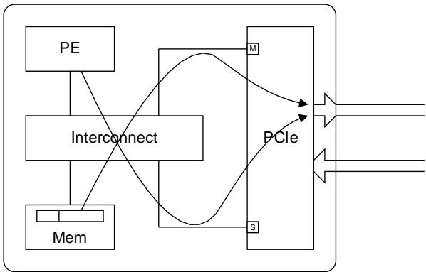
5.4.4.1. Inbound Completion must not overtake Outbound Posted Write [D2]
入站 Completion 不能越过出站 Posted Write
For a Root-SoC only Inbound posted writes and reads need to be considered, therefore the only completion to be considered is that for an Inbound read request.
对于 Root-SoC 而言,仅需考虑入站 posted writes 和 reads,因此唯一需要考虑的完成是针对入站读请求完成。
For an Endpoint-SoC completions for Inbound requests can also include configuration write responses. However, a Configuration Write Completion is permitted to pass a posted write request [rule D2b], so it is also the case that only completions for Inbound read requests needs to be considered when considering ordering.
对于 Endpoint-SoC,入站请求完成也可能包括 Configuration Write 响应。然而,Configuration Write 完成可以允许超越 Posted 写请求 [规则 D2b],因此在考虑排序时,同样只需要考虑入站读请求完成。
For both Root-SoC and Endpoint-SoC the following apply:
- For Inbound completion with
IDO = 0andRO = 0[Rule D2a in the PCIe ordering table]:- The PCIe Interface must not allow the completion for an Inbound read request to overtake an Outbound posted write for which completion response has been returned to the AMBA interconnect.
- For Inbound completion with (
IDO = 0andRO = 1) or (IDO = 1andRO = 1) [Rule D2b in the PCIe ordering table]:- The PCIe interface can allow the completion for an Inbound read request to overtake an Outbound posted write.
- For Inbound completion with
IDO = 1andRO = 0[Rule D2b in the PCIe ordering table]:- Completions for an Inbound read request with
IDO = 1andRO = 0can overtake Outbound posted writes for which a completion response has been returned to the AMBA interconnect provided Requester ID of the posted write and completer ID of the completion are different.
- Completions for an Inbound read request with
对于 Root-SoC 和 Endpoint-SoC,以下规则均适用:
对于 IDO = 0 且 RO = 0 的入站完成 [Rule D2a in the PCIe ordering table]:
- PCIe 接口绝不允许入站读请求的完成超越一个已经向 AMBA 互连返回了完成响应的(BResp)出站 Posted 写。如果 SoC 的内部逻辑认为写操作已经完成,那么它看到的所有后续事件(如这个入站完成)都必须发生在该写操作之后。
对于(IDO = 0 且 RO = 1)或(IDO = 1 且 RO = 1)的入站完成 [Rule D2b in the PCIe ordering table]:
- PCIe 接口可以允许入站读取求的完成超越出站 Posted 写。
对于 IDO = 1 且 RO = 0 的入站完成 [Rule D2b in the PCIe ordering table]:
- 如果已 Posted 写的 Requester ID 与完成的 Completer ID 不同,则 IDO = 1 且 RO = 0 的入站读请求的完成可以超越已向 AMBA 互连返回完成响应(BResp)的出站 Posted 写。
5.4.4.2. Example Use Case
An example of when this is required is a PE in the Root-SoC writing to a data buffer in Endpoint memory using posted writes and this is followed by a write of the valid flag which resides in Root-SoC memory. The PE must only write the valid flag when posted writes to the data buffer are guaranteed to be observed by any agent which can read the valid flag as set.
需要这种排序要求的一个例子是:Root-SoC 中的一个 PE 使用 Posted Writes 向 Endpoint 内存中的 Data Buffer 写入数据,随后再向位于 Root-SoC 内存中的一个有效标志进行写入。该 PE 必须等到对 Data Buffer 的 Posted Writes 能够被任何可能读取到该有效标志置位的 Agent 观察到时,才能写入该有效标志。
The PE that is writing the data buffer using posted writes does not get a guarantee of ordering when the write transaction is accepted. It only gets a guarantee when a write response is given to the posted write. Once the write response has been given by the PCIe interface it is possible that, in a very short period of time, the PE can write the valid flag in Root-SoC memory and this can be read by an Endpoint Inbound read transaction. It is required that the read completion for the transaction from the Endpoint does not overtake the posted writes to the data buffer, so that when the sequence of transactions arrive at the Endpoint the valid flag will only be observed once the writes to the data buffer are guaranteed to be visible. This means that once the Endpoint has received the data for the read of the valid flag it can immediately issue a sequence of reads to obtain the data buffer and it is guaranteed to observe the most recent writes to the buffer.
使用已 Posted 写 Data Buffer 的 PE,在写入事务被 PCIe 接口接受时,并不能获得 Order 的保证。它只有在 PCIe 接口针对该已提交写入给出了一个写入响应(Bresp)后,才能获得 Order 的保证。一旦 PCIe 接口给出了写入响应,PE 就可能在极短的时间内写入位于 Root-SoC 内存中的有效标志,而这个标志可以被一个 Endpoint 的入站读取事务读取。这里的要求是,来自 Endpoint 的这个读取事务的完成绝不能超越对 Data Buffer 的 Posted 写,这样当这一系列事务到达 Endpoint 时,有效标志只有在对 Data Buffer 的写入被保证可见之后才会被观察到。这意味着一旦 Endpoint 收到了读取有效标志的数据,它就可以立刻发出一系列读取来获取 Data Buffer,并且保证能观察到对 Data Buffer 的最新写入。
So, referring back to the original requirements that “Inbound completion must not overtake Outbound posted write request” it can be seen that this can be re-phrased as “A read completion arriving at the PCIe interface from the AMBA interconnect must not be allowed to overtake a write request for which a completion response has been returned.”
因此,回顾最初的要求:“入站完成不能超越出站 Posted 写请求“可以看出,这可以被重新表述为:“一个从 AMBA 互连到达 PCIe 接口的读完成,绝不能被允许超越一个已经返回了完成响应(Bresp)的写入请求。”
Note: Any read completion that arrives before a write response has been given for a posted write does not need to be ordered with respect to that posted write.
For completeness, the same requirements must be observed within an Endpoint-SoC.
The diagram below illustrates this example:
- C1: PE writes to the data buffer in Endpoint-SoC memory.
- P1: The PCIe interface accepts the write to the data buffer, as required by the writes from step C1 and returns a completion response to the PE.
- L1: The posted write to the data buffer is sent across the link first.
- C2: PE writes to set the valid flag in Root-SoC memory.
- E1: Endpoint reads from Root-SoC memory. For this example, it will read the valid flag as set.
- P2: The PCIe reads the valid flag, as required by step E1 and returns the read data, ordered after the earlier posted write.
- L2: The read completion from the valid flag is sent across the link second.
- E2: After the Endpoint agent has completed step E1, it reads the data buffer from Endpoint-SoC memory. It is guaranteed to observe the updated data buffer.
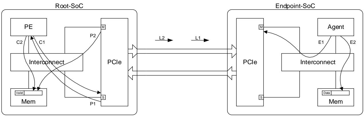
5.4.5. Inbound request/Outbound completion
This describes the ordering requirements of two packets, one is an Inbound transaction request being issued by the PCIe Interface Manager port and the other is the completion for an Outbound request (termed as “Outbound completion”) returning via the PCIe Interface Subordinate port.
- 由 PCIe PCIe Interface Manager 发出的入站事务请求。
- 通过 PCIe Interface Subordinate 返回的、某个出站请求的完成(被称为“出站完成”)。
5.4.5.1. Outbound completion must not overtake Inbound Posted Write. [D2]
出站 Completion 不能越过入站 Posted Write
- For an Outbound completion with
IDO = 0andRO = 0[Rule D2a in the PCIe ordering table]- The PCIe Interface must ensure that an Inbound posted write has received an AXI write completion response before the read data (which is supplied by the completion) for an Outbound read transaction is returned to the requesting agent. This is required when the completion is received after the write request from the PCIe link.
- For an Outbound completion with
IDO = 0andRO = 1orIDO = 1andRO = 1[Rule D2b in the PCIe ordering table]- In this case, the completion can be returned to the requester without waiting for the earlier Inbound posted write to receive its completion response.
- For an Outbound completion with
IDO = 1andRO = 0[Rule D2b in the PCIe ordering table]- In this case, if the Inbound posted write’s Requester ID and the completion’s completer ID are different, then the completion can be returned to the requester without waiting for the earlier Inbound posted write to receive its completion response.
Note that completions for Outbound Configuration writes can overtake Inbound posted write [D2b in the PCIe ordering table].
- 对于 IDO = 0 且 RO = 0 的出站完成 [Rule D2a in the PCIe ordering table]
- PCIe 接口必须确保,在将出站读取事务的读取数据(由出站完成提供)返回给请求方之前,一个入站 Post 写已收到其 AXI 写入完成响应。当该出站完成的接收时间晚于来自 PCIe 链路的写入请求时,此为必要条件。
- 对于 IDO = 0 且 RO = 1 或 IDO = 1 且 RO = 1 的出站完成包 [Rule D2b in the PCIe ordering table]
- 在这种情况下,出站完成可以返回给请求方,无需等待更早的入站 Post 写收到其完成响应。
- 对于 IDO = 1 且 RO = 0 的出站完成包 [Rule D2b in the PCIe ordering table]
- 在这种情况下,如果入站 Post 写的 Requester ID 与该出站完成的 Completer ID 不同,则该出站完成可以返回给请求方,无需等待更早的入站 Post 写收到其完成响应。
注意:出站 Configuration write 的完成可以越过入站 Post 写 [D2b in the PCIe ordering table]。
5.4.5.2. Example Use Case
When considering ordering of completions (which are coming Inbound as a result of Outbound requests) with respect to Inbound transaction requests it is only necessary to consider the relationship between completions for Outbound read requests (i.e. read data returning) and an Inbound posted write.
在考虑完成(Completion)与入站事务请求(Inbound transaction request)的排序时,只需关注出站读请求的完成(即返回的读取数据)与入站 Post 写(Inbound posted write)之间的关系。这里的完成是作为出站请求的响应而入站的。
The requirement is that completions for Outbound read requests (i.e. read data returning) must not overtake an Inbound posted write. In other words, once a PE has received the returning read data it can immediately issue another read transaction and it must be guaranteed to observe the posted write.
具体要求是:出站读请求的完成(即返回的读取数据)不得越过一个入站 Post 写。换言之,一旦 PE 接收到返回的读取数据,它就可以立即发起另一笔读取事务,并且必须保证能够观察到该 Post 写的结果。
An example to illustrate this case is the Endpoint writing a data buffer in Root-SoC memory, using posted writes across the PCIe link followed by a write to set a valid flag which is held in Endpoint memory. When the PE in the Root-SoC attempts to read the valid flag in Endpoint memory it will do so using a read transaction and the returning read data to the PE must force through the posted writes to the data buffer.
为了说明此情况,可以举一个例子:一个 Endpoint 首先通过 PCIe 链路,使用 Post 写将一个 Data Buffer 写入 Root-SoC 的内存中;随后,该 Endpoint 再向其自身的内存中写入一个有效标志位。当 Root-SoC 中的 PE 尝试读取该 Endpoint 内存中的有效标志位时,它会发起一笔读取事务。而返回给 PE 的读取数据(即读完成)必须强制先前发往 Data Buffer 的那些 Post 写先生效
The PCIe Interface must ensure that the earlier posted writes are visible to the PE before the read data is returned. It can do this by ensuring that it has received a write completion response for the posted writes before the read data is returned.
PCIe 接口必须确保,在返回读取数据之前,先前发出的 Post 写对 PE 而言是可见的。实现这一点的机制是:PCIe 接口要确保在返回读取数据之前,已经收到了针对那些 Post 写的写入完成响应(write completion response)。
The diagram below illustrates this example:
- E1: Endpoint agent writes to data buffer in Root-SoC memory.
- E2: Endpoint agent writes to set valid flag in Endpoint-SoC memory.
- C1: PE reads from Endpoint-SoC memory. For this example, it will read the valid flag as set.
- L1: The posted write to the data buffer is sent across the link first.
- L2: The read completion from the valid flag is sent across the link second.
- P1: The PCIe interface writes to the data buffer, as required by the write from step E1.
- P2: The PCIe interface returns the read data, completing step C1, to the PE.
- C2: After PE has completed step C1, it reads the data buffer from Root-SoC memory.
5.5. Ordering and overtaking rules – quick reference
The table below provides a summary of the rules that must be met by a Root-SoC or an Endpoint-SoC with AMBA interconnect for complying with the PCIe ordering model. The “section” column provides a link to the detailed requirements for each rule.
5.6. IDO and RO for Outbound PCIe transactions
This section summarizes IDO and RO setting recommendations for transactions from PE and non-PE agents.
5.6.1. Root-SoC
- For PE generated requests, see 4.7. Setting RO and IDO for PE transactions.
- For requests from non-PE agents (e.g. DMA engines), when to set RO to 1 is IMPLEMENTATION DEFINED.
- For Root-SoC, it is strongly recommended that IDO is not set to 1 for requests from all agents (PE and nonPE) within the Root-SoC. This is because setting IDO for Root-SoC generated transaction is discouraged by the PCIe specification itself.
- For PCIe peer to peer requests being forwarded by the PCIe interface in the Outbound direction, RO and IDO attributes are expected to be supplied by the original requester function.
5.6.2. Endpoint-SoC
- For PE generated requests, see section 4.7. Setting RO and IDO for PE transactions.
- For requests from non-PE agents (e.g. DMA engines), when to set RO to 1 is IMPLEMENTATION DEFINED.
- For requests from non-PE agents in the Endpoint-SoC, when to set IDO to 1 is IMPLEMENTATION DEFINED.
6. Topology Considerations
This section considers some of the topology restrictions that must be observed when integrating PCIe and AMBA systems.
6.1. Bridge Topology Considerations
For the purposes of this discussion a system topology, as shown in the diagram below, is used. This topology has two bridges, Bridge A and Bridge B, on paths that are used for Inbound and Outbound PCI traffic. The bridges are used in the example to allow a discussion of interconnect components that exhibit behaviours. However, a discrete bridge is not required, and the discussion can be applied to any interconnect component.
为了方便讨论,这里使用下图所示的系统拓扑结构。该拓扑结构在用于入站和出站 PCI 流量的路径上有两个桥接器,桥接器 A 和桥接器 B。示例中使用桥接器是为了讨论表现出特定行为的互连组件。然而,并非必须使用独立的桥接器,此讨论可以应用于任何互连组件。
The key features of the system topology are:
- The PCIe Interface Manager port and some other agent, in this case a DMA, share a bridge, Bridge A.
- The PCIe Interface Subordinate port and some other peripherals, in this case a UART, share a bridge, Bridge B.
To avoid deadlock it must be ensured that posted writes are always able to make forward progress.
系统拓扑的主要特性如下:
- PCIe Interface Manager port 和其他代理(在本例中为 DMA)共享一个桥接器,即桥接器 A。
- PCIe Interface Subordinate port 和其他外设(在本例中为 UART)共享一个桥接器,即桥接器 B。
为避免死锁,必须确保 Posted 写操作始终能够向前推进。
6.1.1. Bridge A
It is necessary to ensure that posted writes from PCIe to main memory, path P1, and to peripherals, path P2, can always make forward progress. This must occur whatever traffic is sent by the DMA on path D1.
必须确保从 PCIe 到主内存(路径 P1)和到外设(路径 P2)的 Posted 写始终能够向前推进。无论 DMA 在路径 D1 上发送何种流量,都必须如此。
For a Root-SoC, it is known that all PCIe Inbound write traffic is posted writes, as there cannot be any Inbound configuration writes.
对于 Root-SoC,已知所有 PCIe 入站写流量都是 Posted 写,因为不可能有任何入站 Configuration 写。
DMA reads from PCIe can be blocked. Therefore, it is necessary to ensure that Inbound posted writes from PCIe can always make forward progress, even if reads transactions issued by the DMA are blocked.
DMA 读 PCIe 可能会被阻塞。因此,即使 DMA 发出的读取事务被阻塞,也必须确保来自 PCIe 的入站 Posted 写始终能够向前推进。
If the DMA were capable of issuing configuration writes to PCIe, it would also be necessary to consider the behaviour of the bridge if these writes were not making forward progress. Also, it would be necessary to consider the case where configuration writes were not making forward progress, and this then prevented posted writes which are using the same AXI write channel from making forward progress.
如果 DMA 能够向 PCIe 发出 Configuration 写,则还需要考虑桥接器在这些写未能向前推进时的行为。此外,还需要考虑配置写未能向前推进,并且这会阻止使用相同 AXI 写通道的 Posted 写向前推进的情况。
Ensuring that the bridge has some level of dedicated resource to ensure progress of posted writes from PCIe (or writes in general, if all writes through the bridge can be guaranteed to make forward progress) is recommended.
建议确保桥接器具有一定程度的专用资源,以确保来自 PCIe 的 Posted 写(或一般而言,如果通过桥接器的所有写都可以保证向前推进)的进展。
6.1.2. Bridge B
Bridge B must also ensure that posted writes to PCIe can always make forward progress, even if read transactions to PCIe or configuration writes to PCIe are blocked. In a Root-SoC, support for PCIe peer-to-peer traffic also requires posted writes from the PCIe Interface Manager port to make forward progress to the PCIe Interface Subordinate port.
桥接器 B 还必须确保发往 PCIe 的 Posted 写始终能够向前推进,即使发往 PCIe 的读事务或 Configuration 写被阻塞。在 Root-SoC 中,对 PCIe Peer-to-Peer 流量的支持也要求从PCIe Interface Manager port 发出的 Posted 写能够向前推进到 PCIe Interface Subordinate port。
It is recommended that Bridge B contains dedicated resources for write transactions, to ensure that blocked read transactions do not prevent forward progress of write transactions.
建议桥接器 B 包含用于写事务的专用资源,以确保被阻塞的读取事务不会阻止写事务的向前推进。
In an AXI system, which uses a shared write channel for PCIe posted write transactions and configuration writes, it is necessary to ensure that sufficient resources exist downstream of Bridge B to accept all outstanding configuration writes and ensure that the write channel is not blocked.
在 AXI 系统中,该系统使用共享写通道进行 PCIe Posted 写事务和 Configuration 写,必须确保桥接器 B 下游存在足够的资源来接受所有未完成的 Configuration 写,并确保写通道未被阻塞。
6.2. IO Coherent PCIe Traffic
In a system where the Inbound PCIe traffic is of memory type Outer Shareable WB, it is necessary for snoop transactions to be performed for Inbound posted write transactions. The ACE protocol permits a fully coherent Manager port to stall snoop transactions until earlier write transactions are complete, which could include PCIe posted write transactions and PCIe configuration write transactions.
在入站 PCIe 流量的内存类型为 Outer Shareable WB 的系统中,需要对入站 Posted 写事务执行 Snoop 事务。ACE 协议允许完全一致的管理器端口暂停侦听事务,直到较早的写事务完成,这可能包括 PCIe Posted 写事务和 PCIe 配置写事务。
Therefore, it is necessary for an ACE system to ensure PCIe write transactions can make forward progress. This may require sufficient resources, such as a write buffer, to ensure that it is possible to accept all outstanding configuration writes and ensure that the write channel is not blocked.
因此,ACE 系统必须确保 PCIe 写事务能够向前推进。这可能需要足够的资源,例如 Write Buffer,以确保能够接受所有未完成的 Configuration 写,并确保写通道不会被阻塞。
For a Root-SoC it is permitted to stall Inbound posted write transactions, while Outbound posted write transactions complete. This is required to support peer-to-peer traffic.
对于 Root-SoC,允许暂停入站 Posted 写事务,同时等待出站 Posted 写事务完成。这是支持 Peer-to-Peer 流量所必需的。
However, an Endpoint-SoC is not permitted to stall Inbound posted write transactions while Outbound posted write transactions complete. Therefore, an Endpoint-SoC that requires IO Coherent Inbound traffic must ensure that snoop transactions can always complete without requiring Outbound posted write transactions to complete. This may require sufficient resources to accept all write transactions that could block the progress of snoop transactions for Inbound IO Coherent traffic.
然而,Endpoint-SoC 不允许在出站 Posted 写事务完成时暂停入站 Posted 写事务。因此,需要 IO Coherent 入站流量的 Endpoint-SoC 必须确保 Snoop 事务始终能够完成,而无需等待出站 Posted 写事务完成。这可能需要足够的资源来接受所有可能阻塞入站 IO Coherent 流量的 Snoop 事务进展的写事务。
6.3. Intermediate Components
The traffic from a PCIe Interface may have to pass through intermediate system components before reaching its destination. Two examples of this are:
PCIe 接口的流量在到达目的地之前可能需要通过中间系统组件。两个例子是:
Transactions to memory may pass through a System Memory Management Unit (SMMU), for the purposes of address translation. Interrupt messages may pass through an Interrupt Translation Service (ITS) and Generic Interrupt Controller (GIC), for the purposes of interrupt translation and interrupt delivery.
内存事务可能需要通过系统内存管理单元 (SMMU) 进行地址转换。中断消息可能需要通过中断转换服务 (ITS) 和通用中断控制器 (GIC) 进行中断转换和中断递送。
In both of these cases, and potentially other similar cases, it can be required that the intermediate component must perform read and write accesses to main memory before it can make forward progress on the traffic it is servicing. For example, a read from memory can be required to obtain translation information or a write to memory can be required to update state that is held in a memory-based table.
在这两种情况下,以及其他可能的类似情况下,可能需要中间组件在其处理的流量上取得进展之前,必须对主内存执行读写访问。例如,可能需要从内存中读取以获取转换信息,或者需要写入内存以更新内存表中保存的状态。
To ensure the correct operation of such intermediate components, it is necessary to ensure that these components can access memory without being blocked. This can be achieved using either a dedicated physical channel to memory or a virtual network that provides access to memory that is guaranteed not to be blocked.
为确保此类中间组件的正确运行,必须确保这些组件能够无阻塞地访问内存。这可以通过使用专用的物理内存通道或提供保证不被阻塞的内存访问的虚拟网络来实现。
To ensure that the channel to memory remains free-flowing and is not blocked, it is important to ensure that the channel (either physical or virtual) is not shared with any traffic that may itself need the intermediate component to make forward progress, either directly or indirectly.
为确保内存通道保持自由流动且不被阻塞,重要的是要确保该通道(无论是物理的还是虚拟的)不与任何可能直接或间接需要中间组件才能取得前进的流量共享。
The free-flowing memory traffic must not share a path with:
- Traffic that could itself require the use of the intermediate component.
- Traffic that could be blocked by other traffic that requires the use of the intermediate component.
自由流动的内存流量不得与以下流量共享路径:
- 其本身可能需要使用中间组件的流量。
- 可能被需要使用中间组件的其他流量阻塞的流量。
The following two sections provide examples to illustrate the requirements.
6.3.1. System MMU and PCIe Example
System MMU and PCIe ExampleThe first example, as shown in the diagram below, illustrates the use of a System MMU which is used to provide address translation. The green arrow shows the requirement for a non-blocking path to memory which is used to obtain address translation information. To avoid deadlock this path must not be shared with other traffic that itself has a requirement for the SMMU to make forward progress. In this example, the red arrow shows DMA traffic directed towards PCIe. In order to guarantee forward progress for PCIe Outbound traffic, it is necessary to ensure that Inbound PCIe traffic can make forward progress, and this may require use of the SMMU.Therefore, it is necessary that the SMMU has separate paths for the two traffic types. This can be implemented as separate physical channels or using multiple virtual channels on the same physical wires.
第一个示例,如下图所示,说明了系统 MMU 的使用,该 MMU 用于提供地址转换。绿色箭头表示对内存的非阻塞路径要求,该路径用于获取地址转换信息。为了避免死锁,此路径不得与自身需要 SMMU 才能向前推进的其他流量共享。在此示例中,红色箭头显示了指向 PCIe 的 DMA 流量。为了保证 PCIe 出站流量的向前推进,必须确保入站 PCIe 流量能够向前推进,这可能需要使用 SMMU。因此,SMMU 必须为这两种流量类型提供单独的路径。这可以实现为单独的物理通道,或在同一物理线路上使用多个虚拟通道。
6.3.2. GIC and PCIe Example
The second example, shown below, illustrates a case that needs to be considered when integrating a GIC (Interrupt Controller) with a PCIe Interface. For the purposes of this example, the GIC maintains some state in main memory and therefore must access memory to make forward progress.
The diagram shows traffic from a DMA to the PCIe Interface (red arrow). This traffic, which could be blocked dependent on PCIe Inbound traffic, must not block either of the following:
- GIC traffic (blue arrow) to main memory, which is used to load and store GIC state in which is held in memory-based tables.
- PCIe Interface Inbound traffic, which may be to either the GIC or it could also be to main memory.
The use of separate paths, either separate physical paths or the use of multiple virtual channels on the same physical wires, guarantees forward progress can be made.
第二个示例,如下图所示,说明了在将 GIC(中断控制器)与 PCIe 接口集成时需要考虑的一种情况。为了本示例的目的,GIC 在主内存中维护一些状态,因此必须访问内存才能向前推进。
该图显示了从 DMA 到 PCIe 接口的流量(红色箭头)。这种流量,可能会被 PCIe 入站流量而被阻塞,但它不得阻塞以下任何一种情况:
- GIC 流量(蓝色箭头)到主内存,用于加载和存储 GIC 状态,该状态保存在基于内存的表中。
- PCIe 接口入站流量,可能流向 GIC,也可能流向主内存。
使用单独的路径,无论是单独的物理路径还是在同一物理线路上使用多个虚拟通道,都可以保证向前推进。